Characterizing P2-EVAL Analog Performance
in Propeller 2
Tubular and OzPropDev did some great testing on this a while back (on a P2D2) that’s inspired me to further check out the smart pin-based DAC’s/ADC’s, now on the P2-EVAL board and while using the LDO regulator. Here’s my testing regime:
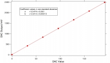
First - I looked at DAC performance in isolation. I connected the DAC output (via a BNC cable - short as possible terminations - from the header pins - P17 and GND) to a 24 bit ADC (on a Linear Technology LTC2448 evaluation board). Means and sdevs of output voltages were then logged at various DAC settings over a 30 second measurement period. P2-EVAL-DACTest.jpg shows the results. The sdev’s on each of these points ranged between 50-70 microvolts. The limited ADC range on the LTC2448 (2.500V) restricted these measurements to DAC<=192. The DAC output was found to be 12.474+12.913(DAC setting) mV; i.e, the DAC has a small offset voltage.
Having established a baseline for DAC performance I then did the following :
Measure and record V1623 (3316 mV) for use in LabVIEW calculations.
(*) Sweep a DAC output on a chosen pin (again I used pin #17) from 0-255 (this pin is connected to an adjacent ADC pin via a shorting header plug).
At each DAC setting, take n readings (here n=2000) each of GIO, PIO and VIO (in sequence) using an ADC channel (here pin #16), setting a fixed period (ADCPER) in smart pin mode 15 and storing each resulting count into HUB RAM.
After said acquisition at each DAC setting, upload HUB to a LabVIEW host vi. This vi plots the respective GIO, PIO and VIO traces, computes n point (PIO-GIO), (VIO-GIO) and ADC result vectors and displays histograms/statistics for each of these parameters. Plots like these are very useful for looking at correlations and revealing underlying issues. In addition, my vi also calculates an effective number of bits (ENOB).
I chose to define ENOB as log2(MEAN[VIO-GIO]) – log2(SDEV[Result]) – this takes into account both the number of bits in the ADC span [VIO-GIO] and the # of bits of noise in the ADC result (which I computed using a 1 sigma measure – of course the ENOB results would be somewhat lower if we were instead to use 2 or 3 sigma). I’m sure the engineering definition of ENOB is different - but the method I’ve described seemed to make intuitive sense.
Store all data/stats into a text file at the current DAC setting and repeat at *
Then - repeat the entire sequence of operations using a new ADC period (ADCPER) setting – here I used values of 2^m with m ranging from 6-16 (i.e ADCPER : 64 – 65536)
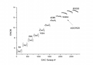
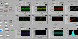
I’ve also attached a screen capture of the vi at the end of the run, the full tab-delimited data file generated and an ENOB plot across the full DAC sweep for each ADCPER value. Approximate achievable sampling rates in these tests – (based on the above 3 point sampling method and ignoring a small ADCPRE acclimation period) - are 1250000/(2^(m-6)) Hz.
In this work my P2 was running at 240 MHz. There’s some interesting (and repeatable) “bowtie” structure in the ENOB traces at the lower ADCPER settings that becomes less pronounced at higher values; in those latter cases ENOB tapers off noticeably as the DAC output approaches VIO. I’m not sure of the reasons for these subtle effects at present. Given that there is some inherent variability in the DAC output on its own as characterized earlier, the actual ADC performance is going to be a little better than what is shown here. One can see that at ADCPER=65536 we are reaching the point of diminishing returns…
Clearly the P2 is offering us considerable flexibility in the ADC speed/resolution trade-off and having 60+ potential analog pins on one chip adds to the wow factor. Sure, there will be more demanding sensors requiring R > 13 bits and for these one will still need to use dedicated high performance ADC’s - but I’ll bet the P2 on its own will cover a large proportion of usage cases.


Comments
For the ENOB graph, the upper right plot points (16384~65536) show deterioration over time, after these plotted in time order? Ie is ENOB getting slightly worse as the chip self-heats? Was this one big long test, or were there gaps between each resolution?
When I did my tests the DACs were unloaded, and I intend to revisit them with the matched load corresponding to each DAC mode, but haven't had time just yet
Also I hope to find out the ADC used in the keysight meter
Really nice to see all that laid out so nicely, well done.
the data presented earlier was one continuous run with each longer ADCPER commenced immediately after the previous. Yes it could be self-heating - did seem likely from your earlier testing - will need to do some more expts (run from cold start, reverse order of tests, lower clock freq etc.)
Nice plots, did that ADC give you a DNL and INL error info or the DACs ?
The bottom axis on the bowtie plots, suggests that is a DAC sweep, so you are showing the ADC (expected-actual) errors across the range ?
That would be expected, as the mid range has the least lower frequency components.
There seem some outlier points (better), only in the first 5, and close to the lower DAC values if I read that right.
Have any worse outlier points been clipped from the graph, as it starts at ENOB appx 5.
50~70µv of variation in DAC, on a fullscale of 2.5V is one part in 35k~50k, so roughly 15 bits
This is where a triangle sweep, of Up and Down on the DAC would help, as on those plots we have both temperature and DAC value increasing.
If L-R is time linear, the slight degrade in ENOB seems to be as one gets closer to the supply voltage.
Running the same test, with a LDO split could be interesting. ie power DAC from one LDO and the ADC from another. That removes a self-tracking artifact that the same-ldo will give.
Did you try lower SysCLKs, to see how much impact a clock change has ?
On the LabVIEW image, there seems one strange artifact in the (VIO-GIO) set.
Notice how the raw values have a different histogram than the voltage corrected ones ? RAW data has a nice single peak, but vcc corrected one has 2 peaks ?
That suggests some rounding error in the calcs, and the mV plot seems to have more definite bands than the raw plot to the left ?
The width of the raw data is roughly +/- 1 part in 2166, but the ENOB reports as 13.2, instead of appx 11 ENOB ?
least 50dB S/N close in for a full amplitude sinewave and no obvious harmonics. IM or multitone
tests I have yet to do, but they usually expose any problems in ac performance.
Thanks for getting into all this.
If anyone has any insight into what we may be able to tweak, in order to improve pertormance, we have a few weeks of time to make small layout changes in.
PLL jitter is the most glaring issue, I think. It needs addressing.
Yes, we need to be able to generate stable video signals that will work reliably.
While you're modifying the PLL, can you make sure that it can run at a higher frequency than the maximum frequency the core can run at? I remember you saying that the PLL fails at a lower frequency than the core, which means that the core is capable of running at a higher frequency but can't because the PLL can't do it, which seems like a waste.
It is nice if it can reach SysCLK max, but also must also be guaranteed to be below the Divider max.
If it can go above SysCLK, you need to be careful the core does not hang, should that happen.
There is something a little strange in the core's clock tolerance, because if you switch the Xtal-source in, before the Xtal has enough amplitude, the P2 will hang.
That may be due to no hysteresis in the Xtal buffer path, with no xtal swing, the amplifier will output whatever it oscillates at in the linear region.
A possible partial fix for that, could be to tweak the bias levels, so the Xtal amplifier DC bias point (nom 50%?) , is not an exact match to the buffer chain bias point.
I'm going to try and capture it with the SLR camera on 1/60 sec but perhaps it would be smarter to use a gopro at 120 or more fps to make sure its only grabbing a single screen at a time
I need to find a way to rule out some other cause eg hsync
Thanks for coming up with that measurement.
So, if we are dividing a 20MHz crystal by 40 to get a 0.5MHz base for multiplication, which results in a 2000ns PFD period, +/-50ns amounts to an uncertainty of about +/-2.5%.
There's an issue with certain temperatures causing jitter to increase, too.
[/quote]
Seems like was fine when divided by 2.
Is 10 MHz not enough granularity?
Yes, there are broadly two different jitter issues.
As Divide increases and PFD falls the general noise loop degrades, and jitter gets worse. eg /64 is proven to have high jitter.
If the jitter crosses the sampling window of the LCD display, it gets amplified to become one pixel.
Keep the PFD high enough, is one rule, but there seems to also be a Temperature zone jitter, which is somewhat nastier, as that can only appear in the field, or perhaps move on a new batch of P2's...
Ah, no, I meant the drift problem. It keeps getting skipped over.
Do you mean ADC drift, that was mostly MHz related from what I recall, and temperature was inferred ?
The raw VIO-GIO histogram in #1, seems to indicate a +/- base width of about one part in 2166, or 11.08 ENOB (which does not match the 2^16 plotted points ?)
The drop in the upper-right plots may be temperature & that slope might be there, but swamped in the lower left by the quantize noise.
(ENOB is a log scale)
Graph0 shows 6 runs, DAC sweeping 0-255 then back down to 0 (i.e. triangle wfm - thanks jmg for the suggestion) while Graph1 shows corresponding ENOB plots for two ADCPER values. Note the nice symmetry here - seems to rule out self-heating (total run time was 3hrs approx @ 240 MHz - x axis - labelled Point # are the successive DAC sweeps and also time advancing).
Re my ENOB values - my calc. method is using a 1 sigma measure for (i.e. just the sdev) of the ADC noise. If the ADC counts are normally distributed then a full width distribution really should be using 3 sigma. Some numbers - an ADC span of 55000 with a signal noise sdev of 6 ADC cts would give ENOB 13.2 but this drops to only 11.5 if one uses 3 sigma. OK - my ENOB's are overly optimistic !
I've found exactly the same shape traces when I run these same tests @ 120 MHz BTW.
I now have a new LV vi so I can vary both the ADC pin (with the DAC pin = ADC pin+1) and sweep the DAC. For some reason I could only look at the even numbered ADC pins (is something wrong with my ADC mode - acdmodpB ??)
In Graph2 I'm scanning through the even numbered ADC pins, outputting fixed DAC=64 on the adjacent pin and measuring 6000 pts of GIO, PIO, VIO, then computing/plotting ENOB. Some pins are clearly doing better than others and that's very evident just looking at the raw data coming back from the ADC.
In Graph3 I've picked out 4 selected ADC/DAC pin pairs and this time ramp through DAC values - starting at 0 in steps of 4 up to 252. One of these pairs was the one investigated in Graph1 (16/17). I repeated the test and have overlaid the two resulting datasets - quite consistent, but slightly different behaviour depending on pin #.
Can't do any more on this now but lots to think about. There's a couple more EVAL boards down here in Melbourne so really need to repeat these measurements early next week with OzPropDev/Tubular to see what we find....