P2 PASM SIN 16Bit
 pic18f2550
Posts: 400
Hello,
is there somewhere a code snippet how I can generate a sinusoidal signal with a 16 bit (smart pin) resolution?
Frequency range 0.001 to 20000.000 Hz.
Thanks
Edit
Back to the actual topic : Sine wave generator.
The file contains a simple example how to build two generators.
The constants "Tabstepp" are dependent on "_clkfreq" & "samp".
I was too lazy to calculate this and just dangled a frequency counter.
Because of the divisions and doubling of the crystal frequency there is always a deviation. With me it was at 20Khz -> 0.02Hz.
The crystal deviation I let times away that is smaller than the grid of the PLL.
Tested with Flexspin.


Comments
Here's something I quickly threw together (and haven't actually tested...) that explains the concept:
              fltl dacpins
              wrpin ##P_DAC_75R_2V|P_OE|P_DAC_DITHER_RND,dacpins ' dac mode
              wxpin ##1000,dacpins ' dac period
              wypin dac_center,dacpins
              outh dacpins
.loop
              testp dacpins wc
        if_nc jmp #.loop
              qrotate dac_center,phase
              add phase,frequency
              getqy tmp
              add tmp,dac_center
              wypin tmp,dacpins
              jmp #.loop

dac_center    long $FF00 / 2
phase         long 0
frequency     long 1<<21
dacpins       long 6 addpins 1 ' pins to output to
tmp           res 1
For more details, read the documentation
Here is aSpin2 example:
https://forums.parallax.com/discussion/comment/1496551/#Comment_1496551
Andy
There is also "headphones.spin2" in Propeller Tools examples. It generates 2 sine waves to 2 pins:
pinbase = 8 left = pinbase+6 right = pinbase+7 freql = 432.0 'left frequency freqr = 440.0 'right frequency volume = $1000 '$0000..$7FFF volume _clkfreq = 256_000_000 dat org asmclk wrpin dac,#left wxpin #256,#left wrpin dac,#right wxpin #256,#right dirh #left addpins 1 setse1 #%001<<6 + left .loop add p1,f1 'calculate right sample qrotate amp,p1 getqx x bitnot x,#15 wypin x,#left add p2,f2 'calculate left sample qrotate amp,p2 getqx x bitnot x,#15 wypin x,#right waitse1 'wait for new period jmp #.loop 'loop x long 0 p1 long 0 p2 long 0 f1 long round(freql * 65536.0 * 65536.0 * 256.0 / float(clkfreq_)) f2 long round(freqr * 65536.0 * 65536.0 * 256.0 / float(clkfreq_)) amp long volume 'dac long %10111_00000000_01_00010_0 'random dither (noisier, needs no period) dac long %10111_00000000_01_00011_0 'pwm (quieter, needs 256N period)I wonder if I have understood this correctly.
2020_03_04
Loop adjusted for the sampelrate.
2020_03_05
Integrated the frequency conversion of the channels.
Note that you don't need (and indeed don't really want) to use WAITCTx to time DAC sampling - Just set the DAC period (Pin's X register) to the desired value and IN will be raised when it is ready for another sample. If you're using multiple DACs, just use the IN from the first one.
Yes, if you start them all up at the same time using ADDPINS, they will forever be synchronized.
Even if they're not started in sync, if you only use the IN from the first one it will also be synchronized, I think.
So I could put wxpin with 192,000.
OK again learned something about it.
Thanks
They will have different phases. The danger is that when you go to update them and you have some timing Jitter, you're getting inconsistent framing, updating some on the intended frame and others on the next frame. If you start them all on the same clock, you have that whole frame. In which to update them all.
---------------------------------------------------------------------
 Syncronisation
---------------------------------------------------------------------
        waitse1                  "wait for new period

---------------------------------------------------------------------
 Ausgabe
---------------------------------------------------------------------
        wypin   x11,#pin1
        wypin   x12,#pin2
        wypin   x13,#pin3
        wypin   x14,#pin4

---------------------------------------------------------------------
 ***
---------------------------------------------------------------------
jmp     #.loop
I don't think the jitters really matter.
The phase offset actuates just 15.625ns per channel.
Yes, in PASM, it is less likely to matter. When it comes to setting unique values, you have no choice.
What is the maximum current carrying capacity of the DAC?
They are resistive, so all currents are a distortion. Highest current would be GIO output at 75 ohm shorted to VIO: 3.3 / 75 = 44 mA. Which is 145 mW heating in a tiny spot.
I expected a little bit.
At 16 bits, the "wxpin # 256, # pin1" should always be the multiple of 256.
With a _clkfreq of 256Mhz I do not get the audio traffic light rate of 192k or 320k.
The values always have a remainder less than 1.
I will have to use "waitct1" again.
The error thus remains below 2 μs.
dat org asmclk ' wrpin dac, #pin1' ' 3 2 1 0' ' 0 0 0 0' ' AAAA_BBBB_FFF_PPP_PP_PPPPPPPP_TT_MMMMM_0' ' 101_VV_DDDDDDDD DAC_MODE (%TT = 00 and %MMMMM = 00000) 8-bit flash, registered' wrpin ##%0000_0000_000_101_00_00000000_00_00000_0,#pin1 'DAC on' ' wxpin #16, #pin1 16 clocks per sample' wxpin #256, #pin1 ' 256 clocks per sample' ' wxpin #4096,#pin1 4096 clocks per sample' '00011 = DAC 16-bit dither, PWM' dirh #pin1 addpins 1 'enable counter' ' setse1 #%001<<6 + pin1 se1 triggers on adc sample' getct t1 .loop add p1,f1 ' 4 calculate sample 1' qrotate amp11,p1 ' 4' getqx x11 ' 4' ' waitse1 4 wait for new period' addct1 t1, s waitct1 wypin x11,#pin1 ' 4 Wert ausgeben' jmp #.loop ' ? loop'How do I switch from DAC to ADC?
I would like to measure the load on the DAC in order to avoid an overload on the DAC.
That enables the DAC with a set value of zero. In that pin mode you have to repeatedly issue WRPIN to set new DAC values. Also, you could use the built in constant for the mode setting, eg: P_DAC_990R_3V
Those are for smartpin control but the smartpin is off. You'd have to set a smartpin mode first, ie: M > 0
This suggests you are desiring the smartpin setup for ADC samples. M = %11000 or P_ADC. In this case the DAC and ADC modes can be combined because only the ADC needs the smartpin. eg: wrpin ##P_DAC_990R_3V | P_ADC, #pin1
Note: To enable the bitstream from the ADC to the smartpin you need to set OUT high.
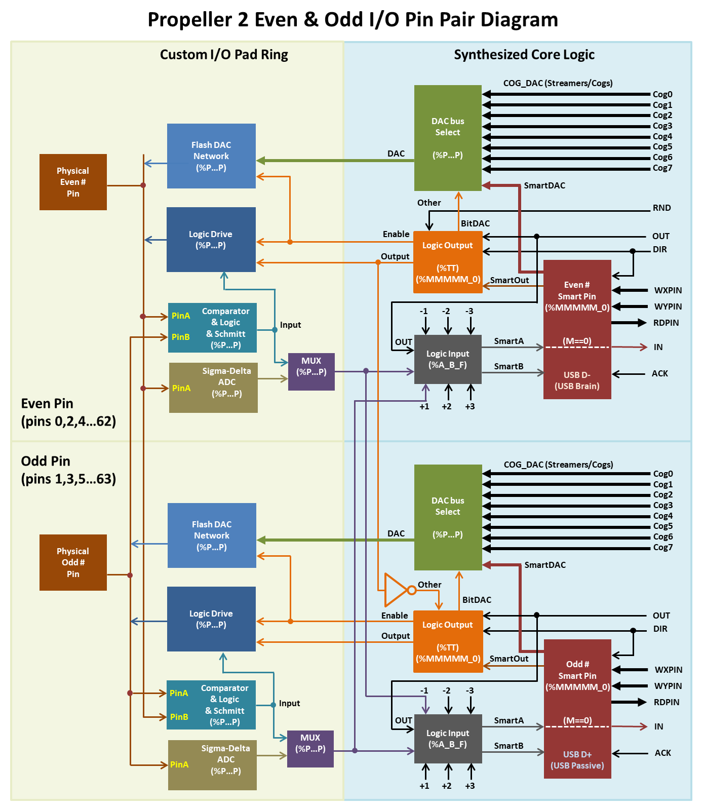
PS: Here's a block diagram of the pin pairs. It shows there is a number of sections involved in using each I/O pin. In your case above you can set the DAC level from the cog through the upper DAC bus select and DAC network sections of the pin diagram ... and at the same time have the smartpin continuously consuming the ADC's bitstream in the lower sections of the pin diagram.

Oh, the mode you're using right now is actually slightly different again, It uses WRPIN instruction for setting DAC level. The block diagram doesn't show the data paths for WRPIN. Instead, the diagram just indicates where each part of the config word is applied block by block.
To use the cog/streamer DAC bus select there is one config bit to set and then you can use SETDACS instruction for updating the DAC level instead of WRPIN.
It's sorta six of one, half a dozen of the other though.
I'll sum up everything I imagine.
The DAC receives a 16bit value from the COG and must output it for an unknown period of time.
The output value of the DAC is read back from the COG via the ADC.
Different COGs will write values to a smartpin "simultaneously" (DAC) and read (ADC).
Is there a document to the PASM commands of the P2?
For spin2 I found something.
A smartpin can only perform one mode at a time. In this case the smartpin is handling the ADC capture.
The DAC is set by the cog directly, bypassing the smartpin. And since the smartpin isn't handling the DAC you also don't get the 16-bit dithered mode, you only get the native 8 bits of the DAC.
You could use two smartpins instead. Have the local smartpin dither the DAC in a smartDAC mode, then have a nearby smartpin routed to this pin's ADC using the %AAAA bits in the "Logic Input" block.
As for simultaneously, it might be a tad fraught. Two cogs accessing the same pin registers on exactly the same clock cycle could be corrupting. Certainly two coinciding WRPINs to the same pin will be a mess. There is a possibility that a RDPIN can reliably coincide with a WXPIN or WYPIN though. I just don't know the details there. I don't remember Chip ever clarifying it.
SETDACS in one cog and RDPIN in another is perfectly okay.
Okay, there is something in the hardware manual but it's less precise than most of Chip's writings. No one's queried Chip on it before it seems.
The first paragraph indicates RDPIN will mess with any coinciding writes ... but the second paragraph also states there is a separate read bus for RDPIN/RQPIN. Which seems to imply a RDPIN can coincide reliably with a WXPIN/WYPIN or even a WRPIN.
Dunno. Still need Chip to clarify.
I can prevent two COGs from accessing the pin at the same time.
What is important is that the values of different COGs are read and written.
I had already guessed that I had to connect two pinns.
Now I have to think a little bit about it.
Hopefully there will soon be a documentary about the P2 PASM like the P1.
The hardware doc is a Google doc, it's the first link of the list here - https://www.parallax.com/propeller-2/documentation/
It can be easy converted to PDF, but the paging isn't very tidy.
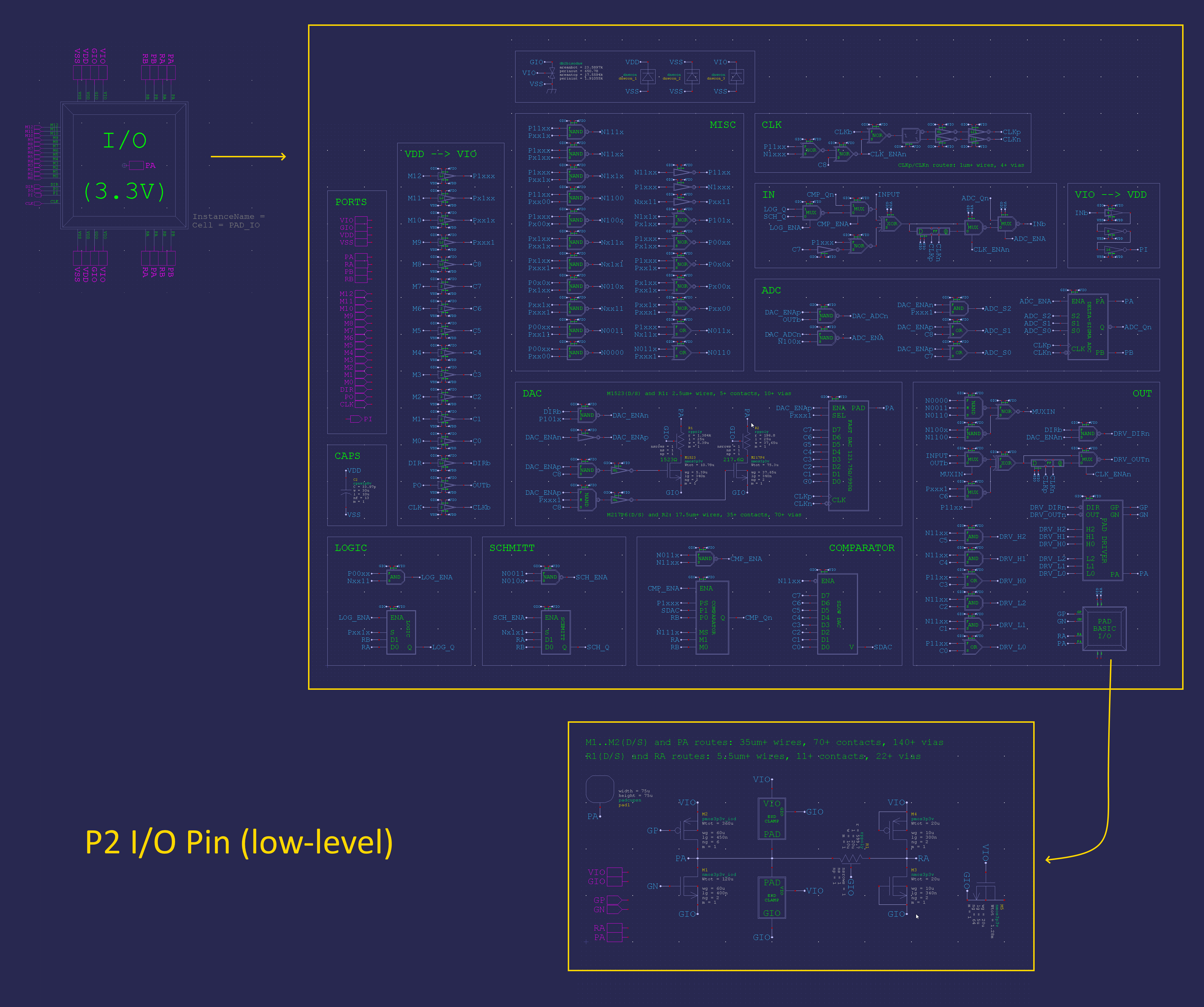
We were able to notably refine the block diagram above when Chip put together a single sheet for us from his I/O pad-ring design files. There was lots of little details like finding out there is an entirely separate DAC for the comparator. And that "input" is muxed with the ADC bitstream after the feedback route.

evanh@
The only thing I can find here is a table with all PASM commands.
I miss some explanation how the commands work.
Or am I just deaf on the eyes?
https://drive.google.com/open?id=1_vJk-Ad569UMwgXTKTdfJkHYHpc1rZwxB-DcIiAZNdk
That's the second link in the list. You probably just mis-clicked. Here's a copy of the correct link https://docs.google.com/document/d/1gn6oaT5Ib7CytvlZHacmrSbVBJsD9t_-kmvjd7nUR6o/edit?usp=sharing
This table has a column called description which expains what the instruction does. It helps if you know a little Verilog for some descriptions. And more complicated instructions are described in the document Evanh has linked.
If both not helps you normally find explanations in this forum with a search. Or just ask.
Here is a good thread:
https://forums.parallax.com/discussion/169069/p2-tricks-traps-differences-between-p1-reference-material-only/p1
Andy
The description is in some cases a little too short.
And Verilog is not exactly my case.
Well, I think I'll have to ask questions here several times.
Googletranslator doesn't make this much better either.