Cluso's NanoBlade2 (digressed to DIP40 discussion)
 Cluso99
Posts: 18,071
Over a year ago I revealed a probable design for a miniature basic P2 pcb.
Now that my RetroBlade2 is running (although not fully tested yet) it is time for my next pcb. The pcb's done and ready to send to production.
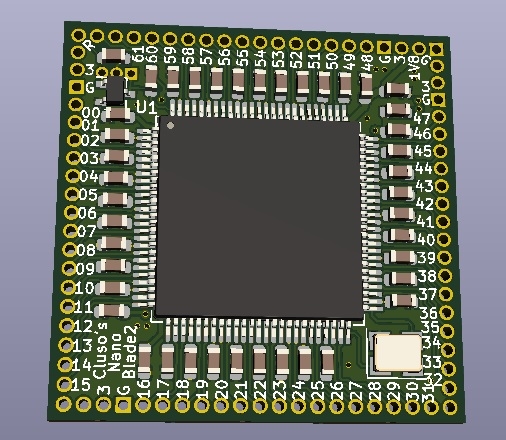
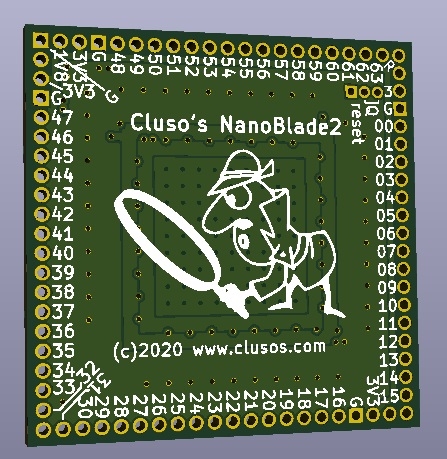
Cluso's P2 NanoBlade2
* PCB 1.08"x1.08" 2 layer ENIG 1.0mm FR4
* P2X8C4M64P chip of course (some initial boards may use P2 RevB chips - let me know if you need RevC)
* 20MHz xtal
* Requires regulated 3V3 and 1V8 (no onboard regulators)
* Proper bulk and bypass capacitors
* Transistor reset circuit (as per P1) configured with solderable link
* 80 pin 0.050" pitch headers around the 4 edges at 1.0" pitch
* All 64 I/O and Reset brought out around the pcb on the 0.050" headers
* Top header has 3V3 and 1V8 plus GND (typically inputs) plus P48-63 and Reset
* Both side and bottom headers have 3V3 and GND (typically outputs) plus P00-15 / P16-31 / P32-47
* No Flash or microSD (basic design only)
* 2x 1x50 0.050" male pin headers supplied but not fitted/soldered
* 3x 1x40 0.050" female pin headers supplied but not fitted/soldered
Note: The pin headers will need to be cut down and filed. Beware if you use the male and female to make a removable pcb - they are difficult to disconnect.


Comments
BTW What dia holes are you using on the microMAT for the 0.050" pads? I've used 0.65mm but wondering if 0.60mm would be tighter but better.
I thought about another pcb to plug into this with the linear regs and maybe the usb-serial (UB2?), flash and microSD. But then that just makes any of other boards which are better suited anyway where that's included.
This was my original (Protel) pcb 1.0"square and 19 pins/side and components both sides. Decided against making this.
Should I make these? Is anyone interested???
No point in doing so just because I can!
You are not going to get it much smaller than the P2D2 or RetroBlade2. So do either of these work for you?
From my perspective, i don’t see the point in a smaller version of the RetroBlade2 as removing the microSD, 2x microUSB and a few IO pins doesn’t really save that much pcb space. I don’t think anything is really missing from your requirements except maybe a reset switch which is easy to add externally if required.
Been thinking some more...
The RetroBlade is 2.2”x1.6”.
By reducing the I/O to 32 (P0-15 and P32-47) with 16 + 3V3 and GND gives 18 pins per side or 1.8” down from 2.2”.
Replacing the microSD with the Flash doesn’t really save any space so the width will need to almost be the same. Perhaps removing the separate 3V3 SOT89 regulator may save 0.2” but there are additional routing issues.
So perhaps a pcb space might get to 1.8”x1.4”. Even squeezing the width a little further maybe 1.8”x1.2” could be optimistic. It’s certainly not going to be a 2.0”x0.6” (pcb 2.0”x0.7”) or even 2.0”x0.9” (pcb 2.0x1.0”) of the DIP40.
It would be easier to make a pcb to go underneath a P2D2 or RetroBlade2 to convert to a DIP40, presuming you are trying to plug into a P1 socket.
I'm not concerned about fitting into a P1 socket, but it would be a nice feature. I think Tubular's design has that feature.
Lachlan’s pcb has the DIP pins located underside and inboard - I think he used another pcb to achieve this???
There are major routing issues in using 0.1” pins and reasonable i/o pin groups to get the minimum width without resorting to 4 layer and/or double sided components both of which add to the cost and complexity.
Using switchers adds to cost and complexity, and probably to ADC noise. Everything is a compromise.
As Peter can attest, placing components on a pcb in no way is routing those components. For instance, the NanoBlade2 is just a cut from the RetroBlade2, but the I/O had to be rerouted. I did this a number of times before it worked. I started with the P2 in the exact center but it wouldn’t route so I had to keep tweeking until it worked - IIRC the P2 is now 7 mils (0.007”) down and 6 mils left from center in order to route the I/O out to the 0.050” pins.
P62-63 would be brought out with Reset and 5V and GND inputs on a separate header. P58-61 would be internal and connected to Flash (no microSD in this case).
P0-15 and P32-47 make the most sense because of the P2 pinout. Would be nicer to have P0-31 but it just doesn’t work.
But the size restriction just doesn’t work
Which is why I ended up with the RetroBlade2 - almost all I/O with 0.1” pins. In the end, microSD and optional VGA connector really didn’t add to the space required.
It’s Chip’s fault - the P2 die and hence TQFP100 package is just too big! He should have left something out haha!
I think you're thinking of the board I showed you a while ago. It doesn't use a second pcb, it uses a special machined header to achieve this. That board width is 0.92" (23mm), because it has to fit in a narrow tube, there simply isn't more width
When I was designing P2-DIP40 I realized its possible to trade P24 for incoming reset (res pin located near P8). This is ok especially when you have a prop plug programmer. However, you lose the ability to program from a legacy P1 DIP40 design, which is my focus, hence that design choice was made
I'll nudge the P2 and post a pic of whats possible in my thread
The pad sizes are 0.583" between outer pads on the TQFP100. If the TQFP is angled, it's even worse. This is without any routing that may take extra space.
- but I'm not sure how important DIP40 form factor is anymore ?
Maybe a FLiP-P2 can upgrade P1 designs to have enough market ?
To the outer end of the P2 pads is 0.583”, then add 2x clearance of 0.005” ( two edges) minimum, then add 2x half the 0.1” pad dia of typ 0.062” which adds up to ~0.655” and you haven’t routed anything, and no bypass caps. Even if you place vias to swap sides, you must add an extra ~ 0.024” + 0.005”.
And if you route all tracks on the underside and inside the P2 pads, the vias have to be staggered inside and you cut down significantly on the ground plane for heat dissipation, and the bypass caps become problematic, as does the 3V3 and 1V8 routing.
But please, don’t let me stop you from making this board
Easy hookup is the key, it doesn't need to plug into the breadboard itself, just jump wires over to one easily if needed.
Never say impossible on this forum.
BTW, I'm not advocating for 0.3". I'm just showing what could be done. 0.6" would make more sense.
Anyone can place components on a 3D model.
But you’ve missed many of the parts you said were required and you’ve only 24 pins for IO and power/ground and reset. Where are the regs and the flash? And that pcb is by my rough guess about 2.1” x 1.0”. And you don’t have proper bulk and bypass caps correctly placed either.
I challenge you to now route that design! That’s the impossible part.
I realize this may be "impossible" for you guys to lay out, but maybe someone else can do it. Tubular is working on something like this, but even more complex since it is a single PCB with multiple pin configurations. I'm just suggesting that I would find a 40-pin (or less) DIP solution useful. It could be plugged into a solderless prototyping board, which could be directly translated to a PCB. There are a lot of hobbyist that prefer to work with 0.1" through-hole parts.
One problem with engineers (me included) is that we think we know what the customer wants rather than listening to them and hearing what they really want. In this case, I'm speaking as a customer and not an engineer.