I guess more explaining is needed ... It's the other way round Tony. In the testing, the streamer's NCO and mode dictates the demand data rate. That's a configured known. What's unknown is the FIFO's behaviour when accessing hubRAM.
So these tests are attempting to measure how often the FIFO bursts hubRAM. And by extrapolation, an average of how much per burst. This is done by setting up the streamer to run continuously at a set rate and then use a SETQ+WRLONG to do a block fill of hubRAM. And measuring how long each block fill takes.
The reasoning is that each time the FIFO accesses hubRAM this stalls the cog's block filling. Because the block writing is in sequential address order this adds 8 clock cycle (tick) increments of time taken to complete the block write. Therefore, the longer the write takes to complete the more often the FIFO made accesses.
The good news is the FIFO can grab a burst of sequential data from hubRAM in one go. This compensates nicely for the fact that the block fill stalls in 8-tick increments. Quote from the silicon doc:
The FIFO contains (cogs+11) stages. When in read mode, the FIFO loads continuously whenever less than (cogs+7) stages are filled, after which point, up to 5 more longs may stream in, potentially filling all (cogs+11) stages.
Each line of the reports has two config parameters:
The streaming data width (column 1)
The NCO increment value (column 3). I've also been calling this the NCO divider, and I note Chip calls it the NCO frequency.
There is a third parameter: The SETQ+WRLONG block writing/filling length, which, above, is set at 64k longwords for all tests. Unimpeded, this takes exactly 65536 ticks to complete.
Okay, so the twelve repeat tests of each line is the measured time taken for a 64k block write to complete.
@jmg said:
What is a 'serious excursion' - does it drop data, or just sometimes take more cycles than hoped ?
...
Things went well until discovery that some streamer rates causes the FIFO to badly hog the hubRAM bus.
What does 'badly hog' amount to ?
With hub being MOD 8, and a NCO not being mod 8, I can see some varying waits could be needed, but things should never 100% choke ?
It's just the time taken, as per the measurements. Chip has wired the FIFO to generally burst 6 longwords from hubRAM at a time. This seems pretty good as it creates an early request condition so that up to 8 longwords can be burst without pushing into a second stall window. The averages should be pretty smooth, and are most of the time.
EDIT: Here's an example with worst case excursions:
BYTE label means the streamer is in RFBYTE mode. For a given streamer NCO rate, when compared to RFLONG, it should only need 1/4 of the bandwidth from hubRAM. So it's to be expected that, for BYTE lines, the block-fill will complete faster than for SHORT or LONG lines. Lower bandwidth should make less bursts. And indeed it is a quicker fill then: 70784 ticks on the BYTE line vs 76936 ticks on the LONG line. Unimpeded being 65536 ticks.
More interesting is that there is no difference between SHORT and LONG. Both take 76936 ticks.
And of course, the eye-popping excursions out to 589760 ticks. Something is going off the rails with those.
EDIT: The SHORT and LONG tests measuring the same were a bug in my code. Now fixed and I've updated the example report snippet above too.
Chip,
Testing is solid now. Conclusion is the FIFO isn't performing optimally on occasion. Certain timings at streamer startup somehow are causing the FIFO to ebb along refilling only 1 - 4 longwords at a time. Or in high volume cases it may sit at 6/12 longwords per refill when multiples of 8 would be far more effective.
Worst case, the FIFO can be hogging 50% of a cog's hubRAM bandwidth while only fetching a single longword every other rotation. EDIT: It might be a lot worse actually. My head is hurting. At any rate, certain combinations should be avoided because of this. Further reading from here - https://forums.parallax.com/discussion/comment/1535820/#Comment_1535820
A detail: This doesn't afflict RFBYTE streamer ops.
EDIT2: Okay, the worst cases are more like 90% hogging and are specifically when the FIFO data rate is either a longword every three sysclock ticks or every nine ticks. Not sure how tight a margin either side of 3 and 9.
Interesting, Evanh. I should have considered, during design, that i> @evanh said:
Chip,
I've before wanted to clarify a particular detail of the cog execution pipeline. In your ASCII art diagram of the pipeline it isn't completely clear at which points cogRAM addressing occurs. Knowing this would clear things up for me.
So, the question is is rdRAM the data from cogRAM ... or is rdRAM the address generation for the next cycle - where data then comes from cogRAM and is subsequently latched?
EDIT: Another way to ask: Where does PC address gen fit into the diagram?
So, rdRAM means that the address is being given to the SRAM to initiate a read cycle. At the end of the next cycle, the read data is captured in a 'latch'.
And wrRAM means that the address and data are being given to the SRAM to initiate a write cycle.
The rdRAM Ix is when the address is given to the SRAM to read the next instruction.
All these rdRAM and wrRAM are clock-edge events where the SRAM latches the address (and data) for a r/w operation that will occur on the next cycle.
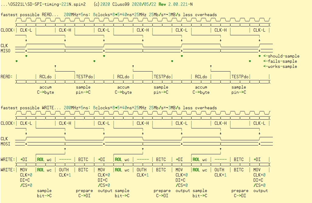
Not bad, but doesn't demonstrate the lag of outputting a SPI clock to SPI data being read back in. As a result the phase alignment of TESTP is etherial.
Also, in reality the sampling alignment arrows need extended more. I would have previously said the OUT latencies was correct but now think they're +1 to what you have. TESTP latencies are also +1 I think.
The combined total, including one for pin slew time, is 8 clock cycles. (From end of OUTx to end of TESTP)
EDIT: Doh! Reading that is tricky. Both Chip and I are working from/to instruction ends. Your one is correct because there is an inbuilt +2 for instruction execution, just needs the +1 added for pin slew.
EDIT2: And when at high sysclock frequencies you can expect an additional +4 from externals.
Chip,
Testing is solid now. Conclusion is the FIFO isn't performing optimally on occasion. Certain timings at streamer startup somehow are causing the FIFO to ebb along refilling only 1 - 4 longwords at a time. Or in high volume cases it may sit at 6/12 longwords per refill when multiples of 8 would be far more effective.
Worst case, the FIFO can be hogging 50% of a cog's hubRAM bandwidth while only fetching a single longword every other rotation. EDIT: It might be a lot worse actually. My head is hurting. At any rate, certain combinations should be avoided because of this. Further reading from here - https://forums.parallax.com/discussion/comment/1535820/#Comment_1535820
A detail: This doesn't afflict RFBYTE streamer ops.
EDIT2: Okay, the worst cases are more like 90% hogging and are specifically when the FIFO data rate is either a longword every three sysclock ticks or every nine ticks. Not sure how tight a margin either side of 3 and 9.
Evanh, I think what is happening is that the FIFO loads all the way up at every opportunity, having priority over RDLONG instructions, and the RDLONG instructions get what's left over. There are some duty relationships between the FIFO loads and RDLONG instructions where the RDLONG is starved more than it would need to be if the FIFO loading was balanced better by having a more complex rule about how much data to read each time it loads. Right now, the rule is that if there's less than a static number of longs in the FIFO, the FIFO loads until that number is reached, after which 5 more longs will stream in because of the clock delays. That logic needs to be improved to fix this problem. That can't happen until we do a silicon respin.
@cgracey said:
... That can't happen until we do a silicon respin.
Putting it on the table for that day.
In last couple days, also noticed that FIFO writes to hubRAM are a lot more hoggie than even the worst case reads. And then worked out this is because the FIFO doesn't explicitly delay its writes. Just has the hub rotation delays.
On the revisit, could also look at adding FIFO delayed write buffering. I know it'd need to auto-flushing after a timeout to keep hubRAM up-to-date.
Ooop, I think I found a technically-not-a-bug-but-really-obnoxious-anyways:
It seems that PUSH/POP do not affect the SKIP suspension counter.
Thus, you can't do the triple tailcall optimization in code that gets called from inside a SKIP sequence.
I.e. turning
call #first
call #second
call #third
ret
into
push #third
push #second
jmp #first
EDIT: oop, double would work, triple and more is the issue.
@rogloh said:
I just tried out the "RET POP D" case to see what would happen. It looks like it returns ok to where it was called from and the D register gets a copy of the return address of the calling code (i.e. caller location in COG RAM + 1), plus the state of the C, Z flags at calling time.
That makes sense. And Chip predicted the same I see.
So if the stack contained both a PUSH'd value as well as the return address ... then the pushed value will become the return address and ... crashie-poo.
@Wuerfel_21 said:
Ooop, I think I found a technically-not-a-bug-but-really-obnoxious-anyways:
It seems that PUSH/POP do not affect the SKIP suspension counter.
Thus, you can't do the triple tailcall optimization in code that gets called from inside a SKIP sequence.
I.e. turning
call #first
call #second
call #third
ret
into
push #third
push #second
jmp #first
EDIT: oop, double would work, triple and more is the issue.
So you'd like to see PUSH/POP increment/decrement skip call counter if it is non-zero?
So you'd like to see PUSH/POP increment/decrement skip call counter if it is non-zero?
Yeah. I don't see any downside to that, since push/pop have to be balanced, anyways.
They don't have to be balanced. A POP when skip call counter is 1 could restart skipping when the intention is not to return to the skip sequence and not to resume skipping. Skip bits could be zeroed in this case.
But that doesn't work as-is, either. It will just continue skipping on the next RET. RETurning from the skip sequence also doesn't work. As-is the skip bits will always be consumed eventually.
Chip,
I've realised there is a problem with the smartpin Sinc2/3 "filter" modes. When a Y parameter is specified all is good and works as expected. But when relying on just the X parameter the decimations from RDPIN are messed up. There is some sort of offset and there is roll-over effects happening too.
I'm of the opinion this should be documented as an errata so people don't try rely on setting the filter modes decimation period using X and instead only use Y for that.
Here's an example that fails because it relies on X for decimation period:
' Program reads an ADC and displays raw count
CON
_clkfreq = 100_000_000 'set clock frequency
DOWNLOAD_BAUD = 230_400
DEBUG_BAUD = DOWNLOAD_BAUD
_pin = 13 'do conversion on this pin
VAR
long reading
long sstack[64]
PUB go()
cogspin( NEWCOG, sampler(), @sstack )
repeat 'print sample set every 100ms
debug(sdec_(reading), dly(100))
PRI sampler() | i, diff
pinstart(_pin, p_adc_3x | p_adc, %1_1100, 0) 'init ADC pin
repeat
if pinread(_pin)
i := rdpin(_pin)
i -= diff
diff += i
reading := i & $7ff_ffff
Change the pinstart to pinstart(_pin, p_adc_3x | p_adc, %1_0000, 4096) and it'll work correctly.
EDIT: Added brackets to COGSPIN's target method to keep Pnut happy. Shows I hadn't tested with Pnut.
Chip,
I got a question regarding smartpins. Hypothetically, for a modified Prop2, based on the existing bus structures, could a selected Z register theoretically be piped into cogRAM space? Have it appear same as the special purpose registers, like INA/INB. I'm thinking this would replace RDPIN in cases where ACK isn't used.
@evanh said:
Chip,
I've realised there is a problem with the smartpin Sinc2/3 "filter" modes. When a Y parameter is specified all is good and works as expected. But when relying on just the X parameter the decimations from RDPIN are messed up. There is some sort of offset and there is roll-over effects happening too.
I'm of the opinion this should be documented as an errata so people don't try rely on setting the filter modes decimation period using X and instead only use Y for that.
Here's an example that fails because it relies on X for decimation period:
' Program reads an ADC and displays raw count
CON
_clkfreq = 100_000_000 'set clock frequency
DOWNLOAD_BAUD = 230_400
DEBUG_BAUD = DOWNLOAD_BAUD
_pin = 13 'do conversion on this pin
VAR
long reading
long sstack[64]
PUB go()
cogspin( NEWCOG, sampler(), @sstack )
repeat 'print sample set every 100ms
debug(sdec_(reading), dly(100))
PRI sampler() | i, diff
pinstart(_pin, p_adc_3x | p_adc, %1_1100, 0) 'init ADC pin
repeat
if pinread(_pin)
i := rdpin(_pin)
i -= diff
diff += i
reading := i & $7ff_ffff
Change the pinstart to pinstart(_pin, p_adc_3x | p_adc, %1_0000, 4096) and it'll work correctly.
EDIT: Added brackets to COGSPIN's target method to keep Pnut happy. Shows I hadn't tested with Pnut.
Thanks, Evanh. So, what we need to document is that when using raw SINC2 or SINC3 modes, you must set the decimation period via WYPIN. Is that right?
@evanh said:
Chip,
I got a question regarding smartpins. Hypothetically, for a modified Prop2, based on the existing bus structures, could a selected Z register theoretically be piped into cogRAM space? Have it appear same as the special purpose registers, like INA/INB. I'm thinking this would replace RDPIN in cases where ACK isn't used.
Yes, that could be done, though timing is tight around the S and D muxes, already.
@evanh said:
Another future feature request: Sync Serial Receiver smartpins get a sync start pattern in Y register. Disabled when Y = 0.
So, it only signals data-received when a certain value arrives. That value would be expressed in the Y register. Maybe an additional bit in the X register could gate this function, so that a full 32-bit value could be set in Y.
@cgracey said:
Thanks, Evanh. So, what we need to document is that when using raw SINC2 or SINC3 modes, you must set the decimation period via WYPIN. Is that right?
@evanh said:
Another future feature request: Sync Serial Receiver smartpins get a sync start pattern in Y register. Disabled when Y = 0.
So, it only signals data-received when a certain value arrives. That value would be expressed in the Y register. Maybe an additional bit in the X register could gate this function, so that a full 32-bit value could be set in Y.
Yep, when the pattern matches then a state change occurs to say everything from now is to be buffered. Prior to the pattern matching the shifter will just keep shifting looking for the pattern to arrive. So the pattern matching is only armed from when DIR gets raised and Y is not 0.
Yeah, I'm open to the pattern being longer than the X value if that's easy to do.
@evanh said:
Chip,
I got a question regarding smartpins. Hypothetically, for a modified Prop2, based on the existing bus structures, could a selected Z register theoretically be piped into cogRAM space? Have it appear same as the special purpose registers, like INA/INB. I'm thinking this would replace RDPIN in cases where ACK isn't used.
Yes, that could be done, though timing is tight around the S and D muxes, already.
Ah, I see. Would want to replace/overlay an existing SPR to keep S/D muxes the same number.
Chip,
Another one for the sync serial smartpins. When operating as master, the clock pin source select would really benefit from using an internal source, rather than having to use an external pin.
The way it currently is makes the rx clock-data relationship surprisingly erratic. This is all about the clock period being shorter than the I/O propagation times of the Prop2 pins. Adjusting the frequency a little can suddenly skip to the next clock pulse for sampling the data pin, meanwhile the slave hasn't shifted its latency.
EDIT: Dunno, maybe this can't be a clean fix. Changing the clock route might just move the erratic nature around a little but not in the end solve anything.
EDIT2: Actually, the tx pin is far worse and is the one that really needs the clock mastering to be internal. Here the I/O propagation hugely creates a lag that otherwise shouldn't exist at all.
EDIT3: Okay, I'm suitably impressed with the sync rx smartpin abilities. It's held up really well. All my issues were stemming from the sync tx smartpin - Which I've now replaced with the streamer for command tx.
Kudos go to the SD card tiny latency as well. I'm pulling 95 MHz SD clock on the command and response and not having to do any dynamic compensation to reliably read back the response via a smartpin. Which means it must be less than 5 ns ... err, or maybe a little more due to the rx smartpin always being another sysclock behind the clock pin ... time to test other SD cards I guess ... All four brands I've got work at 95 MHz!


Comments
I guess more explaining is needed ... It's the other way round Tony. In the testing, the streamer's NCO and mode dictates the demand data rate. That's a configured known. What's unknown is the FIFO's behaviour when accessing hubRAM.
So these tests are attempting to measure how often the FIFO bursts hubRAM. And by extrapolation, an average of how much per burst. This is done by setting up the streamer to run continuously at a set rate and then use a SETQ+WRLONG to do a block fill of hubRAM. And measuring how long each block fill takes.
The reasoning is that each time the FIFO accesses hubRAM this stalls the cog's block filling. Because the block writing is in sequential address order this adds 8 clock cycle (tick) increments of time taken to complete the block write. Therefore, the longer the write takes to complete the more often the FIFO made accesses.
The good news is the FIFO can grab a burst of sequential data from hubRAM in one go. This compensates nicely for the fact that the block fill stalls in 8-tick increments. Quote from the silicon doc:
Each line of the reports has two config parameters:
There is a third parameter: The SETQ+WRLONG block writing/filling length, which, above, is set at 64k longwords for all tests. Unimpeded, this takes exactly 65536 ticks to complete.
Okay, so the twelve repeat tests of each line is the measured time taken for a 64k block write to complete.
It's just the time taken, as per the measurements. Chip has wired the FIFO to generally burst 6 longwords from hubRAM at a time. This seems pretty good as it creates an early request condition so that up to 8 longwords can be burst without pushing into a second stall window. The averages should be pretty smooth, and are most of the time.
EDIT: Here's an example with worst case excursions:
BYTE label means the streamer is in RFBYTE mode. For a given streamer NCO rate, when compared to RFLONG, it should only need 1/4 of the bandwidth from hubRAM. So it's to be expected that, for BYTE lines, the block-fill will complete faster than for SHORT or LONG lines. Lower bandwidth should make less bursts. And indeed it is a quicker fill then: 70784 ticks on the BYTE line vs 76936 ticks on the LONG line. Unimpeded being 65536 ticks.
More interesting is that there is no difference between SHORT and LONG. Both take 76936 ticks.
And of course, the eye-popping excursions out to 589760 ticks. Something is going off the rails with those.
EDIT: The SHORT and LONG tests measuring the same were a bug in my code. Now fixed and I've updated the example report snippet above too.
Chip,
Testing is solid now. Conclusion is the FIFO isn't performing optimally on occasion. Certain timings at streamer startup somehow are causing the FIFO to ebb along refilling only 1 - 4 longwords at a time. Or in high volume cases it may sit at 6/12 longwords per refill when multiples of 8 would be far more effective.
Worst case, the FIFO can be hogging 50% of a cog's hubRAM bandwidth while only fetching a single longword every other rotation. EDIT: It might be a lot worse actually. My head is hurting. At any rate, certain combinations should be avoided because of this. Further reading from here - https://forums.parallax.com/discussion/comment/1535820/#Comment_1535820
A detail: This doesn't afflict RFBYTE streamer ops.
EDIT2: Okay, the worst cases are more like 90% hogging and are specifically when the FIFO data rate is either a longword every three sysclock ticks or every nine ticks. Not sure how tight a margin either side of 3 and 9.
Interesting, Evanh. I should have considered, during design, that i> @evanh said:
So, rdRAM means that the address is being given to the SRAM to initiate a read cycle. At the end of the next cycle, the read data is captured in a 'latch'.
And wrRAM means that the address and data are being given to the SRAM to initiate a write cycle.
The rdRAM Ix is when the address is given to the SRAM to read the next instruction.
All these rdRAM and wrRAM are clock-edge events where the SRAM latches the address (and data) for a r/w operation that will occur on the next cycle.
Excellent. Thanks Chip.
Right, Chip, corrections time. The instruction pipeline graphic in the draft Hardware Manual - https://docs.google.com/document/d/1_b6e9_lIGHaPqZKV37E-MmCvqaS3JKYwCvHEJ-uCq8M/edit?usp=sharing needs corrected to match up with your clarification. There's one too many fetching stages, and it's missing an Execute stage. Also, the stage with MUX is not Store, it is the missing Execute.
Instruction Fetch -> Operands Fetch -> Execute -> Execute -> Store
See my earlier post on alignment of the two ASCII arts - https://forums.parallax.com/discussion/comment/1535164/#Comment_1535164
And the follow on ... because that affects I/O timing via when OUT/DIR registers get updated we then get this:
_____  clk  _____       _____       _____       _____       _____       _____       _____       _____       _____
 -1  |_____|  0  |_____|  1  |_____|  2  |_____|  3  |_____|  4  |_____|  5  |_____|  6  |_____|  7  |_____|  8  |_____|

           |           |    DIRA   |    reg    |    reg    |   P0 OE   |           |           |           |           |
           |           |    OUTA   |    reg    |    reg    |  P0 HIGH  |           |           |           |           |
           |           |           |           |           |  P0 slews |    reg    |    reg    |    INA    |    C/Z    |
           |           |           |           |           |           |           |           |           |           |
     [ DRVH  #0 ]      |           |           |           |           |           |           |     [ TESTP  #0 ]     |
Of note is one less staging register each way than what is shown in the Pin Timing graphics. I've done some testing so feeling cocky.")
EDIT: Made it narrower.
@evanh,
Not sure if this might help....
Thread here
https://forums.parallax.com/discussion/comment/1497556/#Comment_1497556
Not bad, but doesn't demonstrate the lag of outputting a SPI clock to SPI data being read back in. As a result the phase alignment of TESTP is etherial.
Also, in reality the sampling alignment arrows need extended more. I would have previously said the OUT latencies was correct but now think they're +1 to what you have. TESTP latencies are also +1 I think.
The combined total, including one for pin slew time, is 8 clock cycles. (From end of OUTx to end of TESTP)
EDIT: Doh! Reading that is tricky. Both Chip and I are working from/to instruction ends. Your one is correct because there is an inbuilt +2 for instruction execution, just needs the +1 added for pin slew.
EDIT2: And when at high sysclock frequencies you can expect an additional +4 from externals.
I think the hogging is the > @evanh said:
Evanh, I think what is happening is that the FIFO loads all the way up at every opportunity, having priority over RDLONG instructions, and the RDLONG instructions get what's left over. There are some duty relationships between the FIFO loads and RDLONG instructions where the RDLONG is starved more than it would need to be if the FIFO loading was balanced better by having a more complex rule about how much data to read each time it loads. Right now, the rule is that if there's less than a static number of longs in the FIFO, the FIFO loads until that number is reached, after which 5 more longs will stream in because of the clock delays. That logic needs to be improved to fix this problem. That can't happen until we do a silicon respin.
Putting it on the table for that day.
In last couple days, also noticed that FIFO writes to hubRAM are a lot more hoggie than even the worst case reads. And then worked out this is because the FIFO doesn't explicitly delay its writes. Just has the hub rotation delays.
On the revisit, could also look at adding FIFO delayed write buffering. I know it'd need to auto-flushing after a timeout to keep hubRAM up-to-date.
Ooop, I think I found a technically-not-a-bug-but-really-obnoxious-anyways:
It seems that PUSH/POP do not affect the SKIP suspension counter.
Thus, you can't do the triple tailcall optimization in code that gets called from inside a SKIP sequence.
I.e. turning
into
EDIT: oop, double would work, triple and more is the issue.
Unrelatedly: Is
_ret_ pop Dsupposed to work?It seems to work only sometimes, seemingly dependent on what the D address is.
Or maybe I'm just going insane.
/me stirs .. testing time ...
Some of this was discussed before in a related thread...
https://forums.parallax.com/discussion/comment/1491353/#Comment_1491353
Ah, good stuff ...
That makes sense. And Chip predicted the same I see.
So if the stack contained both a PUSH'd value as well as the return address ... then the pushed value will become the return address and ... crashie-poo.
So you'd like to see PUSH/POP increment/decrement skip call counter if it is non-zero?
Yeah. I don't see any downside to that, since push/pop have to be balanced, anyways.
They don't have to be balanced. A POP when skip call counter is 1 could restart skipping when the intention is not to return to the skip sequence and not to resume skipping. Skip bits could be zeroed in this case.
But that doesn't work as-is, either. It will just continue skipping on the next RET. RETurning from the skip sequence also doesn't work. As-is the skip bits will always be consumed eventually.
Chip,
I've realised there is a problem with the smartpin Sinc2/3 "filter" modes. When a Y parameter is specified all is good and works as expected. But when relying on just the X parameter the decimations from RDPIN are messed up. There is some sort of offset and there is roll-over effects happening too.
I'm of the opinion this should be documented as an errata so people don't try rely on setting the filter modes decimation period using X and instead only use Y for that.
Here's an example that fails because it relies on X for decimation period:
' Program reads an ADC and displays raw count

CON
    _clkfreq = 100_000_000                'set clock frequency
    DOWNLOAD_BAUD = 230_400
    DEBUG_BAUD = DOWNLOAD_BAUD

    _pin     = 13                         'do conversion on this pin


VAR
    long    reading
    long    sstack[64]


PUB go()

    cogspin( NEWCOG, sampler(), @sstack )

    repeat                                'print sample set every 100ms
        debug(sdec_(reading), dly(100))


PRI sampler() | i, diff

    pinstart(_pin, p_adc_3x | p_adc, %1_1100, 0)       'init ADC pin

    repeat
        if pinread(_pin)
            i := rdpin(_pin)
            i -= diff
            diff += i
            reading := i & $7ff_ffff
Change the pinstart to
pinstart(_pin, p_adc_3x | p_adc, %1_0000, 4096)and it'll work correctly.EDIT: Added brackets to COGSPIN's target method to keep Pnut happy. Shows I hadn't tested with Pnut.
Chip,
I got a question regarding smartpins. Hypothetically, for a modified Prop2, based on the existing bus structures, could a selected Z register theoretically be piped into cogRAM space? Have it appear same as the special purpose registers, like INA/INB. I'm thinking this would replace RDPIN in cases where ACK isn't used.
Another future feature request: Sync Serial Receiver smartpins get a sync start pattern in Y register. Disabled when Y = 0.
Thanks, Evanh. So, what we need to document is that when using raw SINC2 or SINC3 modes, you must set the decimation period via WYPIN. Is that right?
Yes, that could be done, though timing is tight around the S and D muxes, already.
So, it only signals data-received when a certain value arrives. That value would be expressed in the Y register. Maybe an additional bit in the X register could gate this function, so that a full 32-bit value could be set in Y.
Yes.
Yep, when the pattern matches then a state change occurs to say everything from now is to be buffered. Prior to the pattern matching the shifter will just keep shifting looking for the pattern to arrive. So the pattern matching is only armed from when DIR gets raised and Y is not 0.
Yeah, I'm open to the pattern being longer than the X value if that's easy to do.
Ah, I see. Would want to replace/overlay an existing SPR to keep S/D muxes the same number.
Chip,
Another one for the sync serial smartpins. When operating as master, the clock pin source select would really benefit from using an internal source, rather than having to use an external pin.
The way it currently is makes the rx clock-data relationship surprisingly erratic. This is all about the clock period being shorter than the I/O propagation times of the Prop2 pins. Adjusting the frequency a little can suddenly skip to the next clock pulse for sampling the data pin, meanwhile the slave hasn't shifted its latency.
EDIT: Dunno, maybe this can't be a clean fix. Changing the clock route might just move the erratic nature around a little but not in the end solve anything.
EDIT2: Actually, the tx pin is far worse and is the one that really needs the clock mastering to be internal. Here the I/O propagation hugely creates a lag that otherwise shouldn't exist at all.
EDIT3: Okay, I'm suitably impressed with the sync rx smartpin abilities. It's held up really well. All my issues were stemming from the sync tx smartpin - Which I've now replaced with the streamer for command tx.
Kudos go to the SD card tiny latency as well. I'm pulling 95 MHz SD clock on the command and response and not having to do any dynamic compensation to reliably read back the response via a smartpin. Which means it must be less than 5 ns ... err, or maybe a little more due to the rx smartpin always being another sysclock behind the clock pin ... time to test other SD cards I guess ... All four brands I've got work at 95 MHz!