Shop OBEX P1 Docs P2 Docs Learn Events
Output current of gate driver — Parallax Forums

Output current of gate driver

I am trying 3-phase inverter circuit.

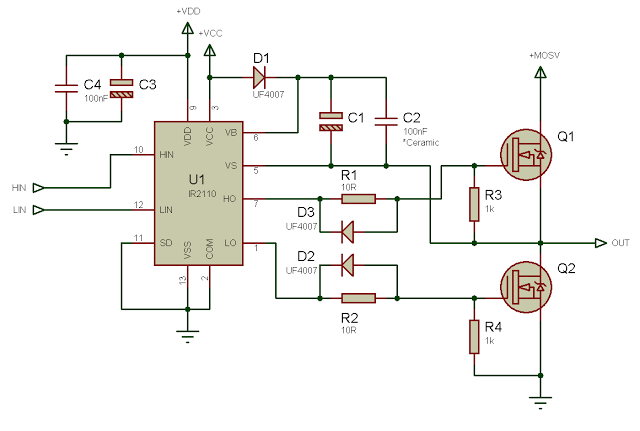
I am using IR2110 to switch high and low side MOSFETs. Each MOSFET's gate is connected to the high/low side pins of driver IC. When I apply the PWM input to the gate driver, the MOSFET switches and the circuit works fine. I connected to the load (motor), the motor runs OK.
When I try to check the gate current of the MOSFET (that is, from driver IC output pin to the MOSFET's gate), I notice that zero amps is flowing to the gate. But how?

I am biasing the gate driver IC with 12 volts and I used a 30 ohm resistor in the gate terminal,
I = 12V/30 = 400mA

But when I measure the current it shows "0 amp". I also changed the value from 30 ohms to 10 ohms. But no change, so I think I am wrong somewhere.
Please correct me.
640 x 431 - 47K
«1

Comments

  • Peter JakackiPeter Jakacki Posts: 10,193
    edited 2018-08-09 07:55
    Of course there is no static drive current due to the very nature of MOSFETs (field-effect) where the gate is an extremely high resistance input except it does have capacitance, which to charge/discharge fast enough to ensure the MOSFET acts as a clean switch (non-linear) requires a driver that can supply that current for the short duration, which may in fact be very repetitive.

    This reminds me of the time a qualified EE thought he found a problem. He said "it must be this NPN transistor, there's only 0.6V on the base" :):):)
  • Heater.Heater. Posts: 21,230
    That's right. Your gates won't see any current except during the very short switching rise and fall times. It's unlikely you will measure that with a multi meter.

    Those gate drives are pulled down with 1K resistors (R3 and R4) so we can expect 12ma of DC current there.

    Sounds like your circuit is working fine.
  • jmgjmg Posts: 15,144
    Budd wrote: »
    But when I measure the current it shows "0 amp". ...

    Using a current probe and a high speed oscilloscope ?
    Average DC current into a Cap load is Zero, but peaks or RMS current will be > 0.

  • tonyp12tonyp12 Posts: 1,950
    edited 2018-08-09 18:31
    Gate drivers, though rated 2Amp they can only provide that for a few micro seconds.
    But that helps with charging and discharing the mosfets capacitive (pF) gate charge very fast
    so the mosfet's transition in the resistive region goes over very fast.

    When turning on/off something like a light/solenoid every other seconds, it does not really matter.
    But a smps powersupply that runs at 1MHz, it does, and also mosfets with low gate charge as the charging and discharging is wasted energy.

    Boot strapping the floating highside does rely on a minimum switching freq, as the mosfets gate charge does dissipates.
    Unlike a dedicated chargepump, boot-strapping needs its capacitor to go from +- to ++ at a minimum external freq to be recharged faster than the mosfets gate field leakage.
  • Thankyou friends.
    I am trying to build a 1KW bldc inverter circuit.
    I used atmel328p processor, gate driver and 12 mosfets. The mosfets swiches good, but when i connected to 1kW motor (at 20v and 10amp supply) the mosfet gets heated up above 60C. The circuit work fine for low watts motors but not for high power motor(1KW).
    I attached the schematic below, correct me friends.
    3120 x 4160 - 1M
    3120 x 4160 - 1M
  • Budd wrote: »
    Thankyou friends.
    I am trying to build a 1KW bldc inverter circuit.
    I used atmel328p processor, gate driver and 12 mosfets. The mosfets swiches good, but when i connected to 1kW motor (at 20v and 10amp supply) the mosfet gets heated up above 60C. The circuit work fine for low watts motors but not for high power motor(1KW).
    I attached the schematic below, correct me friends.

    mosfet=irf3205
  • Are those really plain slow old 1N4007s you are trying to use across the MOSFET? But what MOSFETs are you using. Almost anything will work fine at low switching frequencies but you want fast diodes and fast MOSFETs for high frequency PWM. But I'm not even sure you are trying to control the speed etc. Too little information even though you have diagrams, I would always have a part number for the MOSFETs, not just any old MOSFETs. The charge pump is a bootstrap version so you need to be switching the output continually for it to work. To switchy, no worky.
  • Are those really plain slow old 1N4007s you are trying to use across the MOSFET? But what MOSFETs are you using. Almost anything will work fine at low switching frequencies but you want fast diodes and fast MOSFETs for high frequency PWM. But I'm not even sure you are trying to control the speed etc. Too little information even though you have diagrams, I would always have a part number for the MOSFETs, not just any old MOSFETs. The charge pump is a bootstrap version so you need to be switching the output continually for it to work. To switchy, no worky.

    Mosfet=irf3205, gate driver=ir2110 & switchign freq= 10Khz. I am controlling the speed by changing the duty cycle.
  • Ok, I've used those too but you can leave those diodes out as they are useless and the body diode can handle this easily. Make sure the high-side MOSFET has sufficient drive voltage between gate and source. Best to check this with a scope but of course you can't attach the ground to the source but you can use two probes or just measure Vb with a meter, it needs to be at least 6V or so higher than your Vcc. For a test you can connect another supply to this pin just to rule out the charge pump.
  • Friend i am not having scope, how to measure the Vgs in multi-meter. Because if we measure voltage from mosfets gate to source, it will be wrong right?. Then how to measure the Vgs. And you said that i need to give supply for Vb, already i am biasing Vb by 12v via a in4148
  • Peter JakackiPeter Jakacki Posts: 10,193
    edited 2018-08-15 08:46
    The gate of the MOSFET needs to be several volts higher than the source but your meter can still read the average which should be about half. Don't forget that the AC range is useful here too. However you should be able to read Vb which should have a higher voltage on there.

    The voltage from the diode is insufficient to turn on the high side MOSFET, it simply charges the cap so that when the cap switches it now puts it's voltage in series with the output which if at full voltage would effectively be twice the voltage. It takes a bit of pumping via switching to get there hence the term "charge-pump".

    BTW - a scope is indispensable for anyone designing and testing circuits. Even a pocket scope or a USB scope is affordable.
  • Dude can you explain the explain pump concept. Do you think any changes should me made or additional components is necessary in my circuit side.
  • Heater.Heater. Posts: 21,230
    Imagine you charge up a capacitor with a 9 volt battery.

    Then you disconnected the battery. The capacitor will store the charge for some time. So if you were to measure the voltage across it's terminals you would see about 9 volts.

    Now connect one end of the capacitor to the positive terminal of the battery. Now if you measure the voltage from the other end of the capacitor to the negative end of the battery you will see 18 volts.

    Why?

    Well, the battery delivers 9 volts and the capacitor is charged to 9 volts, in series connection that adds up to 18 volts.

    By making that parallel then series connection you have "pumped" up the voltage available to twice that you started with.

    If you look at the diode capacitor arrangement in your circuit long enough and think about how the voltages change over time and which way currents can or cannot flow you will see that it also pumps up the voltage on the capacitor.

    It's worthwhile doing this experiment for real with a 10uF capacitor and a battery, just to really convince yourself. (Be sure to get electrolytic capacitors the right way around)

  • Heater. wrote: »
    Now connect one end of the capacitor to the positive terminal of the battery. Now if you measure the voltage from the other end of the capacitor to the negative end of the battery you will see 18 volts.

    Why?

    Well, the battery delivers 9 volts and the capacitor is charged to 9 volts, in series connection that adds up to 18 volts.

    By making that parallel then series connection you have "pumped" up the voltage available to twice that you started with.

    That makes the process very clear to me. You learn something new every day!

    Sandy
  • Peter JakackiPeter Jakacki Posts: 10,193
    edited 2018-08-15 13:11
    You need to make sure your components and circuit are working correctly, perhaps you have the wrong part or a bad connection etc. Even a meter should help if you know how and where to use it. Whats voltage are you reading for Vb? It must be several volts higher than your supply voltage otherwise you have a fault somewhere. Of course even if the charge pump wasn't pumping but the diode was ok then it should be very close to the supply voltage.

    BTW Budd - none of us are dudes here on the forum but "Friends" is an ok term although you can even skip that and get straight to what you want to say without embellishments :) .

    Sandy - yeah, and when you put that in series with another cap, and another cap etc you end up "multiplying" the voltage - search "voltage multipliers", they are very similar to charge pumps. Most EEPROM and Flash chips have charge pumps on-chip.
  • Heater. wrote: »
    Imagine you charge up a capacitor with a 9 volt battery.

    Then you disconnected the battery. The capacitor will store the charge for some time. So if you were to measure the voltage across it's terminals you would see about 9 volts.

    Now connect one end of the capacitor to the positive terminal of the battery. Now if you measure the voltage from the other end of the capacitor to the negative end of the battery you will see 18 volts.

    Why?

    Well, the battery delivers 9 volts and the capacitor is charged to 9 volts, in series connection that adds up to 18 volts.

    By making that parallel then series connection you have "pumped" up the voltage available to twice that you started with.

    If you look at the diode capacitor arrangement in your circuit long enough and think about how the voltages change over time and which way currents can or cannot flow you will see that it also pumps up the voltage on the capacitor.

    It's worthwhile doing this experiment for real with a 10uF capacitor and a battery, just to really convince yourself. (Be sure to get electrolytic capacitors the right way around)

    That is what actually bootstrap in gate driver does right? , Your are saying that to reduce 100uf to 10uf.
  • Heater.Heater. Posts: 21,230
    As far as I understand the bootstrap arrangement in the circuit you presented, yes.

    No, I'm not suggesting you change component values in the circuit. They all depend on the actual situation, which I have not analysed at all.

    My 10uf value for an experiment with a capacitor and battery was just an example for such an experiment. Too small and you won't see the effect. To big is not necessary.

    Really, try it for yourself.

  • Peter JakackiPeter Jakacki Posts: 10,193
    edited 2018-08-15 20:12
    Something doesn't seem right, as if somebody else drew out a circuit for you but didn't get it right. Those diodes should be ultra-fast such as UF4007, not 1N4007. If this is an assignment you need to go back and sort it out. I went and perused app notes for this chip and then I tried to find the exact circuit you are using. This is the closest I found and as you can see they use UF4007s but there's also 1k gate to source resistors in there too. But layout is also important and if this is breadboarded then the problem may lay there too. You need to supply a good photo or two in that case.
    This is the circuit I found but there is also another test circuit attached.
    IR2110%20-%202.png
    543 x 575 - 50K
  • tonyp12tonyp12 Posts: 1,950
    edited 2018-08-15 20:54
    boot strap is a simple charge pump, nothing wrong with it but there is some quirks
    It takes one complete cycle to charge up, so you can not start with high side on and leave it there.
    Its voltage doubling buildup dissipates slowly-but-steadily so you need to switch faster than just 1Hz.

    These have build-in bootstrap diode:
    https://www.mouser.com/ProductDetail/STMicroelectronics/L6494LD?qs=sGAEpiMZZMvQcoNRkxSQkrbSyqzE5%2bUqQz2J046wl0c=
    https://www.mouser.com/ProductDetail/Infineon-Technologies/2EDL05N06PJXUMA1?qs=sGAEpiMZZMvQcoNRkxSQkjKGCqEdeY3WnxzpIxXsfEA=

    Nearly all 2-driver IC's use boot strap, it's the 4-driver full h-bridge that I have seen with charge pump to drive N-mosfets on the highside.


  • tonyp12 wrote: »
    boot strap is a simple charge pump, nothing wrong with it but there is some quirks
    It takes one complete cycle to charge up, so you can not start with high side on and leave it there.
    Its voltage doubling buildup dissipates slowly-but-steadily so you need to switch faster than just 1Hz.

    These have build-in bootstrap diode:
    https://www.mouser.com/ProductDetail/STMicroelectronics/L6494LD?qs=sGAEpiMZZMvQcoNRkxSQkrbSyqzE5%2bUqQz2J046wl0c=
    https://www.mouser.com/ProductDetail/Infineon-Technologies/2EDL05N06PJXUMA1?qs=sGAEpiMZZMvQcoNRkxSQkjKGCqEdeY3WnxzpIxXsfEA=

    Nearly all 2-driver IC's use boot strap, it's the 4-driver full h-bridge that I have seen with charge pump to drive N-mosfets on the highside.


    I replaced my 1n4007 with 1n4148(fast swtching diode) and tested for second time, mosfet continue to heats as before.
    - Replaced 1n4007 with 1n4148 across mosfets drain and source.(image attached)
    - But i didn't replace near ic, is it necessary to change near gate driver and mosfet gate.
    - I checked the high side voltage = 10v(between HO pin and gnd) and Vb=20v (@60%duty cycle).
  • Peter JakackiPeter Jakacki Posts: 10,193
    edited 2018-08-16 13:15
    Ok, Vb at 20V sounds good.But fast switching is not the same as fast recovery and a 1N4148 is a signal diode, it's not rated for much power at all. You need a diode that says it is a fast reverse recovery rectifier that's designed for high frequency rectification and also for "freewheeling", that is, those diodes across the MOSFETs although I would think that the MOSFETs body diodes are far better rated for this job.

    But what are you doing trying to get a complicated power circuit working when you're only guessing and you don't even have a scope? No really, I don't understand how you are attempting this and substituting almost any parts like tiny 1N4148 signal diodes in 3-phase inverted circuit, it boggles the mind.
  • We have started this work long before, till now we are working with this inverter circuit. We reached almost to the end but we not completed yet, thought we struggling with this type of small small problems.
    - Ok i will replace with the fast recovery diode
    - DO you think any other cause which leads my fet to heat.
    Friend can you guide me to solve this issue.
  • Heater.Heater. Posts: 21,230
    Budd,
    ...thought we struggling with this type of small small problems....
    My observation is that getting such motor control circuits working is some kind of "rite of passage" for those getting into electronics. The circuits looks so deceptively simple but they are the devil to get working. Often leaving a pile of dead MOSFETs in their wake.

    I'm no great shakes electronics guy but I first observed this back in the early 1980's as an apprentice in a department that did nothing but motor controls.

    Later I myself had a pile of dead MOSFETs whilst trying to build a class D amplifier is a project in technical school.

    So do take the advice that has been offered here. Personally I would start by getting an oscilloscope. It's amazing the capability one can get in a scope for very little money now a days.
  • Heat=power losses in the FET. If I read the specification correctly, Rds was only 0.008 ohm. What are the actual currents through the FET and what are the voltage drops drain to source when operating? What do the gate drive waveforms look like? Is there enough time between pulses to prevent the FETS from having overlapping on times? Or read Taiwan Semiconductor app note AN-1001_A1611. Also another from IR, Power Mosfet Basics which does get into thermal issues. Just some random ideas from a troubleshooting viewpoint.
  • I would struggle with the "small small" problem of reading a voltage if I didn't have a meter.
    I would struggle with the "small small" problem of checking a waveform if I didn't have a scope.

    If I look at the speedo on my car dash I can tell how fast I am going but I need to look out the windscreen to see where I'm going.
    You can't drive a car just by looking at the speedo, you will crash and burn.
    Likewise you can't design and test drive 3-phase inverter switching circuits just by using a meter, because likewise you will crash and burn.
    Beg, borrow, or buy a scope so you can see where you are going wrong or right.

  • evanhevanh Posts: 15,187
    edited 2018-08-17 10:18
    Yes, get a Digital Storage Oscilloscope. And spend lots of time with it.

    Some observations:
    - The hand drawings have problems: 22R resistor between VS and motor phase shouldn't exist. Looks like it's changed to 10R on the other drawing. Get rid of that resistor, the phase wire should be directly to VS (pin 5).

    - Don't use 1N4148 for power rectification! They're only signal diodes. Make sure you use "ultra fast" rectifiers, ie: The UF4007 in the original diagram.

    - As well as gate drive voltage and load current, the gate (dis)charge time is also a major factor in heating consideration. The driver IC (IR2110) is spec'd for 2 A drive strength but the 10R gate series resistors reduce it to maybe 600 mA. That might be a limiting factor for switching speed. It has to overcoming the gate capacitances to perform the switching rapidly.

  • evanhevanh Posts: 15,187
    edited 2018-08-17 13:04
    A heads up on that last point: Gate charge time is affected by load supply voltage. The further Vds has to swing the longer it's capacitance is in opposition to the gate. ie: Vgs flat-lines at the gate switching voltage for the entire switching duration. You can see what voltage that is in figure 6 on page 4 of the IRF3205 datasheet. About 5 volts in this case.

    PS: This is the important Vgs voltage for calculating drive current at.

    EDIT: Added word "supply" to load supply voltage.
  • evanhevanh Posts: 15,187
    Actually, the exact gate switching voltage is a bit more complicated. The load current vs rated Idrain current affect it too. Generally, 4 to 5 volts is it.

  • evanh wrote: »
    Yes, get a Digital Storage Oscilloscope. And spend lots of time with it.

    Some observations:
    - The hand drawings have problems: 22R resistor between VS and motor phase shouldn't exist. Looks like it's changed to 10R on the other drawing. Get rid of that resistor, the phase wire should be directly to VS (pin 5).

    - Don't use 1N4148 for power rectification! They're only signal diodes. Make sure you use "ultra fast" rectifiers, ie: The UF4007 in the original diagram.

    - As well as gate drive voltage and load current, the gate (dis)charge time is also a major factor in heating consideration. The driver IC (IR2110) is spec'd for 2 A drive strength but the 10R gate series resistors reduce it to maybe 600 mA. That might be a limiting factor for switching speed. It has to overcoming the gate capacitances to perform the switching rapidly.
    -Ok evanh, i will replace ultra fast diode.
    - Can you explain me how 600mA will flow, If i use 10R.
    (i,e) I = V/R
    = 12v/10 = 1.2A
    correct me friend if i am wrong.
  • Heater.Heater. Posts: 21,230
    edited 2018-08-20 08:11
    Please read-read my reply to your original post where I mention that.

    Imagine that you removed the MOSFETs from the circuit. Now ask yourself what would be the current flowing out of LO?

    The only current path is down to ground through R2 and R4 in series. That is 10 ohms + 1K ohms = 1010 ohms (this is not just the 10 ohms as you assumed above).

    If LO is high at 12v the the current is I = V/R = 12 /1010 = 11.8811.. ma. Might as well call it 12ma.

    Now put the MOSFETs back into the circuit. The MOSFET gates have very high input impedance, they are effectively just capacitors. So in the DC case they make no difference. The current is still 12ma.

    What about the AC case? Well, those gate capacitors will need current to charge and discharge them as the LO transitions from low to high and high to low respectively. That current is only present during the very brief transition time.

    How big is that current? One could work it out from knowledge of the gate capacitance value. Which I will not get into here. I suspect that the result would be very approximate as that gate capacitance is no doubt changing with voltage and/or current through the device. Also any inductance in the circuit traces will limit the amount of current during these high speed pulses.

    One could measure the gate pulse current by monitoring the voltage across R1 and using Ohms law (We can ignore R4 in this case). For this one will need an oscilloscope. Be sure to make sure the scope is not grounded though.

    Perhaps evanh's guesstimate of 600ma is about correct. I have never looked at this in such detail.

    By the way, in general there is a little trick here to remember. When analyzing a circuit imagine the DC paths and the AC signal paths separately. For the DC paths simply imagine all the capacitors removed. This is what you need to do when assessing bias conditions.


Sign In or Register to comment.