

P2D2 - An open hardware reference design for the P2 CPU
 Peter Jakacki
Posts: 10,193
Peter Jakacki
Posts: 10,193
In the course of documenting the P2 chip I wanted to include some basic schematics but in the process ended up designing a P2 board suitable for P2 development testing and also designing in as a component, hence P2D2, even if it does sound droid.
Why the new thread?
BUT P2D2 is not meant to be a hat or compatible with any other boards, it's main aim is to firstly allow access to all the P2 I/O pins and to have sufficient on-board resources to enable it to run off any USB serial cable. Secondly, it would be compact and versatile enough to mount on a matrix or pcb board as a component for prototypes and low-volume designs. So as to keep all the information and questions about P2D2 from being buried under too many uncontrolled suggestions with their own agenda, I thought I'd start a new thread. Parallax forum etiquette is stacks better than most forums, let's keep it that way.
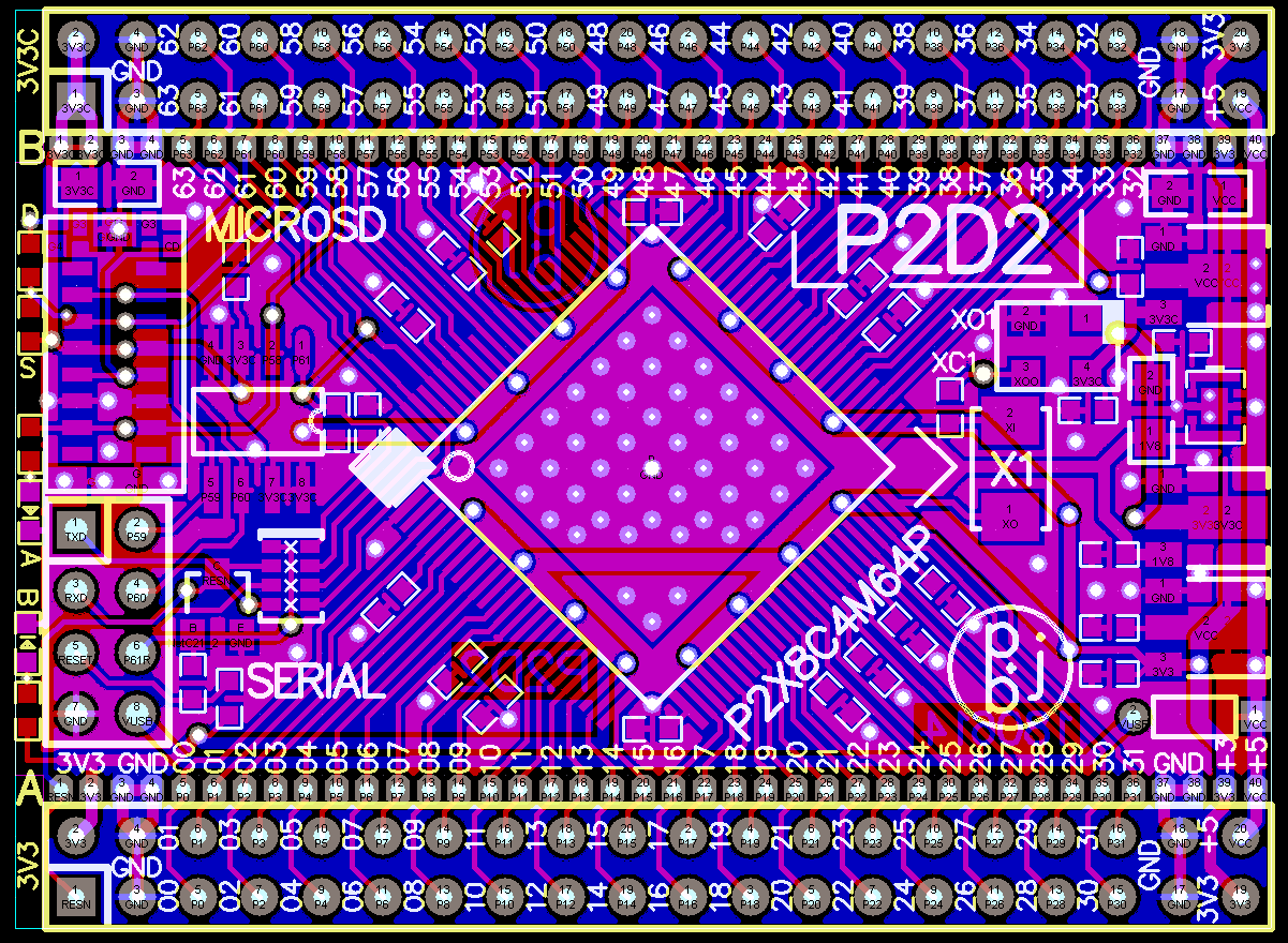
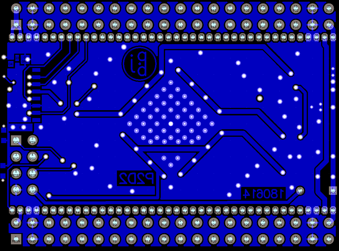
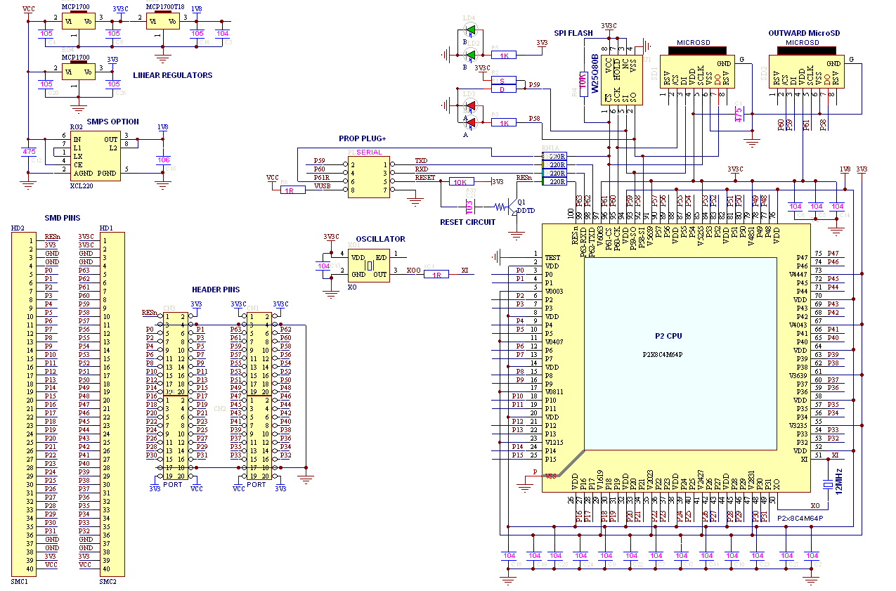
Here are the screenshots of the schematics and pcb layers for reference. This top post will be updated with the current versions and links although the P2D2 document should always be up to date. Look in the dropbox folder for the pcb files which I will try to make available in different formats but if you have successfully imported into your pcb tool and can then export it into other formats then please post those files so that everyone can make use of them.
It is intended that prototypes will be produced before P2 is available so that the circuit can be verified and tested in conjunction with an FPGA board connected to the I/O and reset. Dummy loads will be switched in to test the 3.3 and 1.8V supplies as well. Once P2 chips are available they could be dropped onto a preassembled and tested board.
P2D2 FOLDER
P2D2 DOCUMENT
Updated 180621

Why the new thread?
BUT P2D2 is not meant to be a hat or compatible with any other boards, it's main aim is to firstly allow access to all the P2 I/O pins and to have sufficient on-board resources to enable it to run off any USB serial cable. Secondly, it would be compact and versatile enough to mount on a matrix or pcb board as a component for prototypes and low-volume designs. So as to keep all the information and questions about P2D2 from being buried under too many uncontrolled suggestions with their own agenda, I thought I'd start a new thread. Parallax forum etiquette is stacks better than most forums, let's keep it that way.
Here are the screenshots of the schematics and pcb layers for reference. This top post will be updated with the current versions and links although the P2D2 document should always be up to date. Look in the dropbox folder for the pcb files which I will try to make available in different formats but if you have successfully imported into your pcb tool and can then export it into other formats then please post those files so that everyone can make use of them.
It is intended that prototypes will be produced before P2 is available so that the circuit can be verified and tested in conjunction with an FPGA board connected to the I/O and reset. Dummy loads will be switched in to test the 3.3 and 1.8V supplies as well. Once P2 chips are available they could be dropped onto a preassembled and tested board.
P2D2 FOLDER
P2D2 DOCUMENT
Updated 180621
1201 x 880 - 142K

1193 x 863 - 77K
1177 x 870 - 57K
1275 x 841 - 62K
Comments
Shouldn't there be a pulldown between base emitter on the reset transistor?
BTW I often use a transistor with internal series and pulldown resistors.
Although this is a digital transistor (DDTD) with internal series and pull-down/bias/cutoff resistors you will find that in the early days of germanium transistors especially with their high leakage that this was really really necessary. These days silicon NPN though tends to be low leakage and you need Vbe ~ 0.6V to turn it on anyway.
btw - as a side note, the "cutoff" resistor tends to be used as a voltage divider so that the transistor doesn't even see Vbe(min) until the desired switching voltage is reached. If you don't care and are happy for any voltage >0.6V or so to turn it on then you don't actually need a cutoff, especially if it is also driven low. I'll run LTSpice just to see what it says anyway.
Here it is, just as I said (Sine wave into 2N2222 NPN with 1k series, no cutoff, and 10k load)
btw, I only use 10nF rather than 100nF, so the shorter time constant is more forgiving of a longer discharge cycle. Here are the curves for my circuit showing that even another reset pulse 1ms will still produce a reset, although in regards to the Prop boot timeouts, that wouldn't make any difference even if it did miss it. Certainly though, the second set of curves look better with a 10k pulldown. Over a more realistic time period >30ms however, the curves look the same.
Only thing I noticed was that the capacitor location near pins 48/47 currently looks pretty tight. Depending on how far the P2 pins protrude it just might be very easy to short this cap's ground to pin 47 when you get your iron tip in if your board is hand soldered due to the 0.5mm pitch of the P2 (I think it is 0.5mm right?). The other one near pins 15/16 doesn't look quite as cramped. A simple remedy may be to just shrink down the pin number silk in size a fraction in order to push the cap further away or even just overlap the silk a tad.
I'm thinking of trying out that JCL PCB place next week for some early protos and I will make sure I send you guys some boards.
No problems and I really do welcome critique
I intend to load a right angle dual row pin header for the serial since vertical is so limited but right angle sits flat and allows entry through the side of a case.
The microSD connector is available in various heights but the one I use allows a card to slide nicely across the top of the P2 straight into the socket. I've done the same before with P1 so I know it works nicely. There is a footprint for an outward facing connector on the reverse side in case I would like external access. I think the mechanicals should be fine but that's also one of the reasons to get early protos since they are cheap enough to "print".
btw - here's a screenshot of the 3D model of the microSD connector that I use:
This is a nice board with everything accessible. Great for checking out the P2. It's small enough, yet has the ability to connect to expansion boards, which you can make yourself. I bet Peter will make some too.
I will be sending the artwork off for blank pcbs next week and will probably have quite a few spare to hand out although for anyone else to assemble if they want. Obviously if the P2 chip checks out then this would be a good board to check it out on but I will have to think about making assembled units for sale.
Might just be my graphic editing software but it seemed to be slightly out, but perhaps not enough to make any real difference.
I note though, that the MCP1700 is rated 200 mA. I think there was mention of possibly 2 watts max needed on the 1.8 volt rail. I get the feeling that even if the XCL220 was in place, even its 1 amp rating would be too low.
That would allow the board to be more conveniently used with two 1x20 SIL headers fitted on the extreme edges for use with breadboard or stripboard, would give full access to all power rails, access to all even numbered I/O pins.
@evanh - MCP1700 part# is mainly a placeholder and while I do use these regs I note that there are many options in the same package up to 1A such as the AZ1117R but even the AP7365 handles 600ma at the cost of 21 cents in 100's. The XCL220 is priced at around $1.80 and while it may be true that even its 1A rating might not be enough, at the same time I'm not too fussed either as I don't think we would be pushing every cog at maximum, at least for now, plus I could assist the switcher with the LDO possibly or feed 1.8V externally. However, I'd hate to think of the P2 consuming all that power as it does seem excessive.
@T Chap - The "parallel" LEDs are only in the schematic as it is a mounting option to have them on top or on the reverse in case this board is flipped.
@hippy - Here is a composite view on a 0.1" grid:
It's a Molex 47309-2651
Here's a Mouser link
As Ken has stated, until P2 is "real" they can't and don't want to commit precious resources to it as they need to focus on business so that there is a business there to support P2 (my own words). But obviously Parallax made up the 123 boards to support P2 so I guess they would do the same for the chip itself. I'm intending to send Chip some of these boards (if he wants them) made up ready to tack a P2 onto if he wants to, but that's totally up to him, I'm just trying to be helpful and show my appreciation. I guess too that the Protel99SE pcb format is easily handled by its successor, Altium, so that they could use that as a basis for an in-house board too.
@evanh - To dress up some boards I have these neat outlines on the silk to identify different sections and if I have the room for it I will add what I can but the you've got to remember that the board is quite small and even though they can print idents a lot finer these days, they might still be a bit hard to see on anything other than the blown-up artwork.
Don't worry, I don't have a problem with making a small run of them as they are fairly simple but obviously I'd only make enough first up to test P2 and if all's well, then I can run off 10-20 units or as necessary when some more chips are available. Remember that only a few P2 die will be packaged for testing first up and if that's a go then we will have to wait on the remainder of that batch to be packaged and sent across, and of those I'm sure Parallax will want quite a few for testing variations etc.
Here's the latest top view with the P2 and microSD for scale.
I've done some small 0.5mm stuff before by hand (mainly FFC connectors), though I can't really say I enjoyed it with my eyes as I don't really have a decent or well lit magnification setup. It's a good test of your hand-eye coordination though.
I only moved the cap by 5mil
You will find that trying to hand solder fine pitch simply with a very fine tip can be a very frustrating experience since the fine tip will not conduct sufficient heat to the mass of pad and pin and solder. If I have to hand solder fine pitch I will tack the component down first and then blob on fresh solder "across" all the pins with a warm iron, hot enough to make it blob but not hot enough to burn off the flux. I then turn up the iron, wait until it's hot, and then holding the pcb at an angle I run the broad flat tip along the pins letting the solder melt properly and balling onto the tip as I run it down and veer off at the last pad with the blob of solder on the tip (watch your bare legs). If some pads are bridged, no problem, run the flux gel down the pins and with a clean tip repeat the exercise and you will have a row of very neat and cleanly soldered fine pitch pins. The mass and shape of the broad flat tip helps to hold and conduct the heat as well as attract and hold the mass of excess solder. Easy peasy.