

SDram_Controller --- Question to Chip?
 Sapieha
Posts: 2,964
Sapieha
Posts: 2,964
Hi Chip.
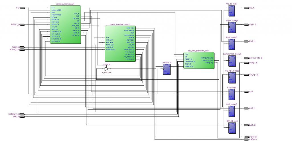
As I don't understand Yours control of SDRAM.
I have one question if You look on posted files and describe how much Yours control difer from that?
Ps This modules don't use Alteras code and use no more that about 350 LTE's
As I don't understand Yours control of SDRAM.
I have one question if You look on posted files and describe how much Yours control difer from that?
Ps This modules don't use Alteras code and use no more that about 350 LTE's

Comments
My laptop is not letting me open those files tonight. Meanwhile, my big, fast desktop has Windows 8 on it, and it has never liked the internet for more than 15 seconds at a time, once every month, or so. I don't even ask why, anymore.
Would you be able to extract the verilog and put it into a code window in this thread? It shouldn't be more than a page or two of code.
Thanks.
http://support.microsoft.com/kb/2832566
Massimo
I think you mean an Upgrade to more functionality
The whole SDRAM driver is software-based... HW are only the registered outputs, as far as I know...
use 7zip to open them http://www.7-zip.org/
All files needed to compile it to look as JPG file in first post.
FILES attached.
Top file -- sdr_sdram.v
/******************************************************************************
*
*  LOGIC CORE:          SDR SDRAM Controller
*  MODULE NAME:         sdr_sdram()
*  COMPANY:             Northwest Logic, Inc.
*                       [URL="http://www.nwlogic.com"]www.nwlogic.com[/URL]
*
*  REVISION HISTORY:
*
*    Revision 1.0  05/11/2000     Description: Initial Release.
*             1.1  07/10/2000     Description: change precharge to terminate
*                                              for full page accesses.
*
*  FUNCTIONAL DESCRIPTION:
*
*  This module is the top level module for the SDR SDRAM controller.
*
*  Copyright Northwest Logic, Inc., 2000.  All rights reserved.
******************************************************************************/
module sdr_sdram(
        CLK,
        RESET_N,
        ADDR,
        CMD,
        CMDACK,
        DATAIN,
        DATAOUT,
        DM,
        SA,
        BA,
        CS_N,
        CKE,
        RAS_N,
        CAS_N,
        WE_N,
        DQ,
        DQM
        );


`include        "params.v"

input                           CLK;                    //System Clock
input                           RESET_N;                //System Reset
input   [`ASIZE-1:0]            ADDR;                   //Address for controller requests
input   [2:0]                   CMD;                    //Controller command
output                          CMDACK;                 //Controller command acknowledgement
input   [`DSIZE-1:0]            DATAIN;                 //Data input
output  [`DSIZE-1:0]            DATAOUT;                //Data output
input   [`DSIZE/8-1:0]          DM;                     //Data mask input
output  [11:0]                  SA;                     //SDRAM address output
output  [1:0]                   BA;                     //SDRAM bank address
output  [1:0]                   CS_N;                   //SDRAM Chip Selects
output                          CKE;                    //SDRAM clock enable
output                          RAS_N;                  //SDRAM Row address Strobe
output                          CAS_N;                  //SDRAM Column address Strobe
output                          WE_N;                   //SDRAM write enable
inout   [`DSIZE-1:0]            DQ;                     //SDRAM data bus
output  [`DSIZE/8-1:0]          DQM;                    //SDRAM data mask lines

reg     [11:0]                  SA;                     //SDRAM address output
reg     [1:0]                   BA;                     //SDRAM bank address
reg     [1:0]                   CS_N;                   //SDRAM Chip Selects
reg                             CKE;                    //SDRAM clock enable
reg                             RAS_N;                  //SDRAM Row address Strobe
reg                             CAS_N;                  //SDRAM Column address Strobe
reg                             WE_N;                   //SDRAM write enable

reg     [`DSIZE-1:0]            DQIN;
wire    [`DSIZE-1:0]            DQOUT;
wire    [`DSIZE-1:0]            IDATAOUT;                //Data output
reg     [`DSIZE-1:0]            DATAOUT;                 //Data output

wire    [11:0]                  ISA;                     //SDRAM address output
wire    [1:0]                   IBA;                     //SDRAM bank address
wire    [1:0]                   ICS_N;                   //SDRAM Chip Selects
wire                            ICKE;                    //SDRAM clock enable
wire                            IRAS_N;                  //SDRAM Row address Strobe
wire                            ICAS_N;                  //SDRAM Column address Strobe
wire                            IWE_N;                   //SDRAM write enable

wire    [`ASIZE-1:0]            saddr;
wire    [1:0]                   sc_cl;
wire    [1:0]                   sc_rc;
wire    [3:0]                   sc_rrd;
wire                            sc_pm;
wire    [3:0]                   sc_bl;
wire                            load_mode;
wire                            nop;
wire                            reada;
wire                            writea;
wire                            refresh;
wire                            precharge;
wire                            oe;

//wire                            CLK133;
//wire                            CLK133B;
//wire                         CLK;


//pll1 PLL1(
//                .inclock(CLK),
//                .clock0(CLK133),
//                .clock1(CLK133B),
//                .locked(locked)
//                );


control_interface control1 (
            //    .CLK(CLK133),
                .CLK(CLK),
                .RESET_N(RESET_N),
                .CMD(CMD),
                .ADDR(ADDR),
                .REF_ACK(ref_ack),
                .CM_ACK(cm_ack),
                .NOP(nop),
                .READA(reada),
                .WRITEA(writea),
                .REFRESH(refresh),
                .PRECHARGE(precharge),
                .LOAD_MODE(load_mode),
                .SADDR(saddr),
                .SC_CL(sc_cl),
                .SC_RC(sc_rc),
                .SC_RRD(sc_rrd),
                .SC_PM(sc_pm),
                .SC_BL(sc_bl),
                .REF_REQ(ref_req),
                .CMD_ACK(CMDACK)
                );

command command1(
               // .CLK(CLK133),
                .CLK(CLK),
                .RESET_N(RESET_N),
                .SADDR(saddr),
                .NOP(nop),
                .READA(reada),
                .WRITEA(writea),
                .REFRESH(refresh),
                .PRECHARGE(precharge),
                .LOAD_MODE(load_mode),
                .SC_CL(sc_cl),
                .SC_RC(sc_rc),
                .SC_RRD(sc_rrd),
                .SC_PM(sc_pm),
                .SC_BL(sc_bl),
                .REF_REQ(ref_req),
                .REF_ACK(ref_ack),
                .CM_ACK(cm_ack),
                .OE(oe),
                .SA(ISA),
                .BA(IBA),
                .CS_N(ICS_N),
                .CKE(ICKE),
                .RAS_N(IRAS_N),
                .CAS_N(ICAS_N),
                .WE_N(IWE_N)
                );

sdr_data_path data_path1(
                //.CLK(CLK133),
                .CLK(CLK),
                .RESET_N(RESET_N),
                .OE(oe),
                .DATAIN(DATAIN),
                .DM(DM),
                .DATAOUT(IDATAOUT),
                .DQIN(DQIN),
                .DQOUT(DQOUT),
                .DQM(DQM)
                );


always @(posedge CLK)
begin
                SA      <= ISA;
                BA      <= IBA;
                CS_N    <= ICS_N;
                CKE     <= ICKE;
                RAS_N   <= IRAS_N;
                CAS_N   <= ICAS_N;
                WE_N    <= IWE_N;
                DQIN    <= DQ;
                DATAOUT <= IDATAOUT;
end

assign  DQ = oe ? DQOUT : 32'bz;

endmodule
File 2: -- sdr_data_path.v
/******************************************************************************
*
*  LOGIC CORE:          SDR Data Path Module
*  MODULE NAME:         sdr_data_path()
*  COMPANY:             Northwest Logic, Inc.
*                       www.nwlogic.com
*
*  REVISION HISTORY:
*
*    Revision 1.0  05/11/2000     Description: Initial Release.
*             1.1  07/10/2000     Description: change precharge to terminate
*                                              for full page accesses.
*  FUNCTIONAL DESCRIPTION:
*
*  This module is the data path module for the SDR SDRAM controller.
*
*  Copyright Northwest Logic, Inc., 2000.  All rights reserved.
******************************************************************************/
module sdr_data_path(
        CLK,
        RESET_N,
        OE,
        DATAIN,
        DM,
        DATAOUT,
        DQIN,
        DQOUT,
        DQM
        );

`include        "params.v"

input                           CLK;                    // System Clock
input                           RESET_N;                // System Reset
input                           OE;                     // Data output(to the SDRAM) enable
input   [`DSIZE-1:0]            DATAIN;                 // Data input from the host
input   [`DSIZE/8-1:0]          DM;                     // byte data masks
output  [`DSIZE-1:0]            DATAOUT;                // Read data output to host
input   [`DSIZE-1:0]            DQIN;                   // SDRAM data bus
output  [`DSIZE-1:0]            DQOUT;
output  [`DSIZE/8-1:0]          DQM;                    // SDRAM data mask ouputs
//reg     [`DSIZE-1:0]            DATAOUT;
reg     [`DSIZE/8-1:0]          DQM;

// internal
reg     [`DSIZE-1:0]            DIN1;
reg     [`DSIZE-1:0]            DIN2;

reg     [`DSIZE/8-1:0]          DM1;


reg     [`DSIZE-1:0]            DOUT1;
reg     [`DSIZE-1:0]            DOUT2;


// Allign the input and output data to the SDRAM control path
always @(posedge CLK or negedge RESET_N)
begin
        if (RESET_N == 0)
        begin
                DIN1    <= 0;
                DIN2    <= 0;
                DM1     <= 0;
                DOUT1   <= 0;
                DOUT2   <= 0;
        end

        else
        begin
                DIN1      <= DATAIN;
                DIN2      <= DIN1;

                DM1       <= DM;
                DQM       <= DM1;


//                DOUT1     <= DQIN;
//                DATAOUT   <= DQIN;


        end
end

//assign  DQ = OE ? DIN2 : 32'bz;
assign DQOUT = DIN2;
assign DATAOUT = DQIN;

endmodule
File 3: -- PLL1.V
// megafunction wizard: %ALTCLKLOCK%
// GENERATION: STANDARD
// VERSION: WM1.0
// MODULE: altclklock

// ============================================================
// File Name: PLL1.v
// Megafunction Name(s):
//             altclklock
// ============================================================
// ************************************************************
// THIS IS A WIZARD-GENERATED FILE. DO NOT EDIT THIS FILE!
// ************************************************************


//Copyright (C) 1991-2000 Altera Corporation
//Any megafunction design, and related net list (encrypted or decrypted),
//support information, device programming or simulation file, and any other
//associated documentation or information provided by Altera or a partner
//under Altera's Megafunction Partnership Program may be used only to
//program PLD devices (but not masked PLD devices) from Altera.  Any other
//use of such megafunction design, net list, support information, device
//programming or simulation file, or any other related documentation or
//information is prohibited for any other purpose, including, but not
//limited to modification, reverse engineering, de-compiling, or use with
//any other silicon devices, unless such use is explicitly licensed under
//a separate agreement with Altera or a megafunction partner.  Title to
//the intellectual property, including patents, copyrights, trademarks,
//trade secrets, or maskworks, embodied in any such megafunction design,
//net list, support information, device programming or simulation file, or
//any other related documentation or information provided by Altera or a
//megafunction partner, remains with Altera, the megafunction partner, or
//their respective licensors.  No other licenses, including any licenses
//needed under any third party's intellectual property, are provided herein.
`timescale 1 ps / 1 ps

module pll1 (
    inclock,
    locked,
    clock0,
    clock1);
/* synthesis black_box */
    input      inclock;
    output      locked;
    output      clock0;
    output      clock1;

/* synopsys translate_off */
    wire  sub_wire0;
    wire  sub_wire1;
    wire  sub_wire2;
    wire  clock0 = sub_wire0;
    wire  clock1 = sub_wire1;
    wire  locked = sub_wire2;

    altclklock    altclklock_component (
                .inclock (inclock),
                .clock0 (sub_wire0),
                .clock1 (sub_wire1),
                .locked (sub_wire2));
    defparam
        altclklock_component.inclock_period = 7500,                 /* 133mhz */
//        altclklock_component.inclock_period = 10000,                /* 100mhz */
        altclklock_component.clock0_boost = 1,
        altclklock_component.clock1_boost = 1,
        altclklock_component.operation_mode = "NORMAL",
        altclklock_component.valid_lock_cycles = 5,
        altclklock_component.invalid_lock_cycles = 5,
        altclklock_component.valid_lock_multiplier = 5,
        altclklock_component.invalid_lock_multiplier = 5,
        altclklock_component.clock0_divide = 1,
        altclklock_component.clock1_divide = 1,
        altclklock_component.outclock_phase_shift = 0;

/* synopsys translate_on */
endmodule

// ============================================================
// CNX file retrieval info
// ============================================================
// Retrieval info: PRIVATE: DISPLAY_FREQUENCY STRING "25.0"
// Retrieval info: PRIVATE: USING_FREQUENCY NUMERIC "0"
// Retrieval info: PRIVATE: DEVICE_FAMILY NUMERIC "1"
// Retrieval info: PRIVATE: FEEDBACK_SOURCE NUMERIC "1"
// Retrieval info: PRIVATE: PHASE_UNIT NUMERIC "0"
// Retrieval info: PRIVATE: USING_PROGRAMMABLE_PHASE_SHIFT NUMERIC "1"
// Retrieval info: CONSTANT: INCLOCK_PERIOD NUMERIC "40000"
// Retrieval info: CONSTANT: CLOCK0_BOOST NUMERIC "1"
// Retrieval info: CONSTANT: CLOCK1_BOOST NUMERIC "1"
// Retrieval info: CONSTANT: OPERATION_MODE STRING "NORMAL"
// Retrieval info: CONSTANT: VALID_LOCK_CYCLES NUMERIC "5"
// Retrieval info: CONSTANT: INVALID_LOCK_CYCLES NUMERIC "5"
// Retrieval info: CONSTANT: VALID_LOCK_MULTIPLIER NUMERIC "5"
// Retrieval info: CONSTANT: INVALID_LOCK_MULTIPLIER NUMERIC "5"
// Retrieval info: CONSTANT: CLOCK0_DIVIDE NUMERIC "1"
// Retrieval info: CONSTANT: CLOCK1_DIVIDE NUMERIC "1"
// Retrieval info: CONSTANT: OUTCLOCK_PHASE_SHIFT NUMERIC "0"
// Retrieval info: USED_PORT: inclock 0 0 0 0 INPUT NODEFVAL inclock
// Retrieval info: USED_PORT: locked 0 0 0 0 OUTPUT NODEFVAL locked
// Retrieval info: USED_PORT: clock0 0 0 0 0 OUTPUT NODEFVAL clock0
// Retrieval info: USED_PORT: clock1 0 0 0 0 OUTPUT NODEFVAL clock1
// Retrieval info: CONNECT: @inclock 0 0 0 0 inclock 0 0 0 0
// Retrieval info: CONNECT: locked 0 0 0 0 @locked 0 0 0 0
// Retrieval info: CONNECT: clock0 0 0 0 0 @clock0 0 0 0 0
// Retrieval info: CONNECT: clock1 0 0 0 0 @clock1 0 0 0 0
File 4: -- control_interface.v
/******************************************************************************
*
*  LOGIC CORE:          Control Interface - Top level module
*  MODULE NAME:         control_interface()
*  COMPANY:             Northwest Logic, Inc.
*                       www.nwlogic.com
*
*  REVISION HISTORY:
*
*    Revision 1.0  05/11/2000     Description: Initial Release.
*             1.1  07/10/2000     Description: change precharge to terminate
*                                              for full page accesses.
*
*  FUNCTIONAL DESCRIPTION:
*
*  This module is the command interface module for the SDR SDRAM controller.
*
*  Copyright Northwest Logic, Inc., 2000.  All rights reserved.
******************************************************************************/
module control_interface(
        CLK,
        RESET_N,
        CMD,
        ADDR,
        REF_ACK,
        CM_ACK,
        NOP,
        READA,
        WRITEA,
        REFRESH,
        PRECHARGE,
        LOAD_MODE,
        SADDR,
        SC_CL,
        SC_RC,
        SC_RRD,
        SC_PM,
        SC_BL,
        REF_REQ,
        CMD_ACK
        );

`include        "params.v"

input                           CLK;                    // System Clock
input                           RESET_N;                // System Reset
input   [2:0]                   CMD;                    // Command input
input   [`ASIZE-1:0]            ADDR;                   // Address
input                           REF_ACK;                // Refresh request acknowledge
input                           CM_ACK;                 // Command acknowledge
output                          NOP;                    // Decoded NOP command
output                          READA;                  // Decoded READA command
output                          WRITEA;                 // Decoded WRITEA command
output                          REFRESH;                // Decoded REFRESH command
output                          PRECHARGE;              // Decoded PRECHARGE command
output                          LOAD_MODE;              // Decoded LOAD_MODE command
output  [`ASIZE-1:0]            SADDR;                  // Registered version of ADDR
output  [1:0]                   SC_CL;                  // Programmed CAS latency
output  [1:0]                   SC_RC;                  // Programmed RC delay
output  [3:0]                   SC_RRD;                 // Programmed RRD delay
output                          SC_PM;                  // programmed Page Mode
output  [3:0]                   SC_BL;                  // Programmed burst length
output                          REF_REQ;                // Hidden refresh request
output                          CMD_ACK;                // Command acknowledge


reg                             NOP;
reg                             READA;
reg                             WRITEA;
reg                             REFRESH;
reg                             PRECHARGE;
reg                             LOAD_MODE;
reg     [`ASIZE-1:0]            SADDR;
reg     [1:0]                   SC_CL;
reg     [1:0]                   SC_RC;
reg     [3:0]                   SC_RRD;
reg     [3:0]                   SC_BL;
reg                             SC_PM;
reg                             REF_REQ;
reg                             CMD_ACK;

// Internal signals
reg                             LOAD_REG1;
reg                             LOAD_REG2;
reg     [15:0]                  REF_PER;
reg     [15:0]                  timer;
reg                             timer_zero;


// Command decode and ADDR register
always @(posedge CLK or negedge RESET_N)
begin
        if (RESET_N == 0)
        begin
                NOP             <= 0;
                READA           <= 0;
                WRITEA          <= 0;
                REFRESH         <= 0;
                PRECHARGE       <= 0;
                LOAD_MODE       <= 0;
                SADDR           <= 0;
        end

        else
        begin

                SADDR <= ADDR;                                  // register the address to keep proper
                                                                // alignment with the command

                if (CMD == 3'b000)                              // NOP command
                        NOP <= 1;
                else
                        NOP <= 0;

                if (CMD == 3'b001)                              // READA command
                        READA <= 1;
                else
                        READA <= 0;

                if (CMD == 3'b010)                              // WRITEA command
                        WRITEA <= 1;
                else
                        WRITEA <= 0;

                if (CMD == 3'b011)                              // REFRESH command
                        REFRESH <= 1;
                else
                        REFRESH <= 0;

                if (CMD == 3'b100)                              // PRECHARGE command
                        PRECHARGE <= 1;
                else
                        PRECHARGE <= 0;

                if (CMD == 3'b101)                              // LOAD_MODE command
                        LOAD_MODE <= 1;
                else
                        LOAD_MODE <= 0;

                if ((CMD == 3'b110) & (LOAD_REG1 == 0) & (CMD_ACK == 0))                              //LOAD_REG1 command
                        LOAD_REG1 <= 1;
                else
                        LOAD_REG1 <= 0;

                if ((CMD == 3'b111) & (LOAD_REG2 == 0) & (CMD_ACK == 0))                              //LOAD_REG2 command
                        LOAD_REG2 <= 1;
                else
                        LOAD_REG2 <= 0;

        end
end


// register configuration information if LOAD_REG1 or LOAD_REG2 is
// asserted.
always @(posedge CLK or negedge RESET_N)
begin

        if (RESET_N == 0)
        begin
                SC_CL   <= 0;
                SC_RC   <= 0;
                SC_RRD  <= 0;
                SC_PM   <= 0;
                SC_BL   <= 0;
                REF_PER <= 0;
        end

        else
        begin
                if (LOAD_REG1 == 1)
                begin
                        SC_CL   <= SADDR[1:0];                   // CAS Latency
                        SC_RC   <= SADDR[3:2];                   // RC delay
                        SC_RRD  <= SADDR[7:4];                   // RRD delay
                        SC_PM   <= SADDR[8];                     // Page Mode
                        SC_BL   <= SADDR[12:9];                  // Burst length
                end

                if (LOAD_REG2 == 1)
                        REF_PER <= SADDR[15:0];                  // REFRESH Period

        end
end


//  Generate CMD_ACK
always @(posedge CLK or negedge RESET_N)
begin
        if (RESET_N == 0)
                CMD_ACK <= 0;
        else
                if (((CM_ACK == 1) | (LOAD_REG1 == 1) | (LOAD_REG2 == 1)) & (CMD_ACK == 0))
                        CMD_ACK <= 1;
                else
                        CMD_ACK <= 0;
end


// refresh timer


always @(posedge CLK or negedge RESET_N) begin
        if (RESET_N == 0)
        begin
                timer           <= 0;
                timer_zero      <= 0;
                REF_REQ         <= 0;
        end

        else
        begin
                if (timer_zero == 1)
                        timer <= REF_PER;
                else if (SC_BL != 0)
                        timer <= timer - 1;
                if ((timer==0) & (SC_BL != 0))
                begin
                        timer_zero <= 1;
                        REF_REQ    <= 1;
                end

                else
                if (REF_ACK == 1)
                begin
                        timer_zero <= 0;
                        REF_REQ    <= 0;
                end
        end
end

endmodule
File 5: -- altclklock.v
// megafunction wizard: %ALTCLKLOCK%
// GENERATION: STANDARD
// VERSION: WM1.0
// MODULE: altclklock

// ============================================================
// File Name: PLL1.v
// Megafunction Name(s):
//             altclklock
// ============================================================
// ************************************************************
// THIS IS A WIZARD-GENERATED FILE. DO NOT EDIT THIS FILE!
// ************************************************************


//Copyright (C) 1991-2000 Altera Corporation
//Any megafunction design, and related net list (encrypted or decrypted),
//support information, device programming or simulation file, and any other
//associated documentation or information provided by Altera or a partner
//under Altera's Megafunction Partnership Program may be used only to
//program PLD devices (but not masked PLD devices) from Altera.  Any other
//use of such megafunction design, net list, support information, device
//programming or simulation file, or any other related documentation or
//information is prohibited for any other purpose, including, but not
//limited to modification, reverse engineering, de-compiling, or use with
//any other silicon devices, unless such use is explicitly licensed under
//a separate agreement with Altera or a megafunction partner.  Title to
//the intellectual property, including patents, copyrights, trademarks,
//trade secrets, or maskworks, embodied in any such megafunction design,
//net list, support information, device programming or simulation file, or
//any other related documentation or information provided by Altera or a
//megafunction partner, remains with Altera, the megafunction partner, or
//their respective licensors.  No other licenses, including any licenses
//needed under any third party's intellectual property, are provided herein.
`timescale 1 ps / 1 ps

module altclklock (
    inclock,
//    inclocken,
//    fbin,
    locked,
    clock0,
    clock1);

/* synthesis black_box */

    input      inclock;
//    input      inclocken;
//    input      fbin;
    output      locked;
    output      clock0;
    output      clock1;

/* synopsys translate_off*/


parameter inclock_period=7500;                    // 133mhz
//parameter inclock_period=10000;                    // 100mhz
parameter inclock_settings = "UNUSED";
parameter valid_lock_cycles = 3;
parameter invalid_lock_cycles = 3;
parameter valid_lock_multiplier = 1;
parameter invalid_lock_multiplier = 1;
parameter operation_mode = "NORMAL";
parameter clock0_boost = 2;
parameter clock0_divide = 1;
parameter clock1_boost = 1;
parameter clock1_divide = 1;
parameter clock0_settings = "UNUSED";
parameter clock1_settings = "UNUSED";
parameter outclock_phase_shift = 0;


reg clock0, clock1, locked;
reg new_clock0, new_clock1, locked_int;
reg start_new_clock0, start_new_clock1, outclock_start_edge;
reg first_clock0_cycle, first_clock1_cycle;
reg prev_inclock;
wire inclocken;
// internal reg

integer pll0_half_period, pll1_half_period, phase_delay0, phase_delay1;
integer inclock_edge_count;
real lowcycle, highcycle;
reg  cycleviolation;


initial
begin
  locked_int = 0;
  inclock_edge_count = 0;
  first_clock0_cycle = 1;
  first_clock1_cycle = 1;
  lowcycle = 0;
  highcycle = 0;
  cycleviolation = 0;
end

assign inclocken = 1;
always @ (inclock /*or inclocken*/)
begin
   if (locked_int == 0) begin
      pll0_half_period = (inclock_period * clock0_divide)/(2 * clock0_boost);
      pll1_half_period = (inclock_period * clock1_divide)/(2 * clock1_boost);
//      if (outclock_phase_shift < 180.000) begin
         outclock_start_edge = 1;
//         phase_delay0 = (0.500 - (outclock_phase_shift/360.000)) * (2.000 * pll0_half_period);
//         phase_delay1 = (0.500 - (outclock_phase_shift/360.000)) * (2.000 * pll1_half_period);
//     end

//      else if (outclock_phase_shift == 180.000) begin
//         outclock_start_edge = 0;
//         phase_delay0 = (outclock_phase_shift/360.000) * (2.000 * pll0_half_period);
 //        phase_delay1 = (outclock_phase_shift/360.000) * (2.000 * pll1_half_period);
  //    end

   //   else begin
    //     outclock_start_edge = 0;
     //    phase_delay0 = ((outclock_phase_shift/360.000) - 0.500) * (2.000 * pll0_half_period);
      //   phase_delay1 = ((outclock_phase_shift/360.000) - 0.500) * (2.000 * pll1_half_period);

   //   end
      phase_delay0 = outclock_phase_shift;
      phase_delay1 = outclock_phase_shift;
      start_new_clock0 = outclock_start_edge;
      start_new_clock1 = !outclock_start_edge;
   end

   if ((inclocken == 0) || (cycleviolation == 1)) begin
      inclock_edge_count = 0;
      locked_int = 0;
      locked = 0;
   end
   else if  (inclock != prev_inclock) begin // inclock edge detected
      if (inclock == 1) begin
         if (($realtime - lowcycle) != (inclock_period/2)) begin
            $display ($time, "Error: Duty Cycle violation");
            cycleviolation = 1;
         end
         highcycle = $realtime;
      end
      if (inclock == 0) begin
         if (($realtime - highcycle) != (inclock_period/2)) begin
            $display ($time, "Error: Duty Cycle violation");
            cycleviolation = 1;
         end
         lowcycle = $realtime;
      end
      inclock_edge_count = inclock_edge_count + 1;
      if (inclock_edge_count == valid_lock_cycles) begin
         cycleviolation = 0;
         locked_int = 1;
         locked = 1;
      end
   end

    prev_inclock = inclock;
end

always @ (new_clock0 or locked_int)
begin
      if (locked_int == 1) begin
         if (first_clock0_cycle == 1) begin
            clock0 = start_new_clock0;
             # phase_delay0 new_clock0 <= ~start_new_clock0 ;
         end
         else begin
            clock0 = new_clock0;
            # (pll0_half_period) new_clock0 <= ~new_clock0 ;
         end
         first_clock0_cycle = 0;
      end
      else begin
         first_clock0_cycle = 1;
      end
end

always @ (new_clock1 or locked_int)
begin
      if (locked_int == 1) begin
         if (first_clock1_cycle == 1) begin
            clock1 = start_new_clock1;
            #phase_delay1 new_clock1 <= ~start_new_clock1 ;
         end
         else begin
            clock1 = new_clock1;
            # (pll1_half_period) new_clock1 <= ~new_clock1 ;
         end
         first_clock1_cycle = 0;
      end
      else begin
         first_clock1_cycle = 1;
      end
end
//synopsys translate_on
endmodule


// ============================================================
// CNX file retrieval info
// ============================================================
// Retrieval info: PRIVATE: DISPLAY_FREQUENCY STRING "25.0"
// Retrieval info: PRIVATE: USING_FREQUENCY NUMERIC "0"
// Retrieval info: PRIVATE: DEVICE_FAMILY NUMERIC "1"
// Retrieval info: PRIVATE: FEEDBACK_SOURCE NUMERIC "1"
// Retrieval info: PRIVATE: PHASE_UNIT NUMERIC "0"
// Retrieval info: PRIVATE: USING_PROGRAMMABLE_PHASE_SHIFT NUMERIC "0"
// Retrieval info: CONSTANT: INCLOCK_PERIOD NUMERIC "40000"
// Retrieval info: CONSTANT: CLOCK0_BOOST NUMERIC "1"
// Retrieval info: CONSTANT: CLOCK1_BOOST NUMERIC "1"
// Retrieval info: CONSTANT: OPERATION_MODE STRING "EXTERNAL_FEEDBACK"
// Retrieval info: CONSTANT: VALID_LOCK_CYCLES NUMERIC "5"
// Retrieval info: CONSTANT: INVALID_LOCK_CYCLES NUMERIC "5"
// Retrieval info: CONSTANT: VALID_LOCK_MULTIPLIER NUMERIC "5"
// Retrieval info: CONSTANT: INVALID_LOCK_MULTIPLIER NUMERIC "5"
// Retrieval info: CONSTANT: CLOCK0_DIVIDE NUMERIC "1"
// Retrieval info: CONSTANT: CLOCK1_DIVIDE NUMERIC "1"
// Retrieval info: USED_PORT: inclock 0 0 0 0 INPUT NODEFVAL inclock
// Retrieval info: USED_PORT: locked 0 0 0 0 OUTPUT NODEFVAL locked
// Retrieval info: USED_PORT: inclocken 0 0 0 0 INPUT NODEFVAL inclocken
// Retrieval info: USED_PORT: fbin 0 0 0 0 INPUT NODEFVAL fbin
// Retrieval info: USED_PORT: clock0 0 0 0 0 OUTPUT NODEFVAL clock0
// Retrieval info: USED_PORT: clock1 0 0 0 0 OUTPUT NODEFVAL clock1
// Retrieval info: CONNECT: @inclock 0 0 0 0 inclock 0 0 0 0
// Retrieval info: CONNECT: locked 0 0 0 0 @locked 0 0 0 0
// Retrieval info: CONNECT: @inclocken 0 0 0 0 inclocken 0 0 0 0
// Retrieval info: CONNECT: @fbin 0 0 0 0 fbin 0 0 0 0
// Retrieval info: CONNECT: clock0 0 0 0 0 @clock0 0 0 0 0
// Retrieval info: CONNECT: clock1 0 0 0 0 @clock1 0 0 0 0
File 6: -- Command.v
/****************************************************************************** * * LOGIC CORE: Command module * MODULE NAME: command() * COMPANY: Northwest Logic Design, Inc. * www.nwlogic.com * * REVISION HISTORY: * * Revision 1.0 05/11/2000 Description: Initial Release. * 1.1 07/10/2000 Description: change precharge to terminate * for full page accesses. * * FUNCTIONAL DESCRIPTION: * * This module is the command processor module for the SDR SDRAM controller. * * Copyright Northwest Logic, Inc., 2000. All rights reserved. ******************************************************************************/ module command( CLK, RESET_N, SADDR, NOP, READA, WRITEA, REFRESH, PRECHARGE, LOAD_MODE, SC_CL, SC_RC, SC_RRD, SC_PM, SC_BL, REF_REQ, REF_ACK, CM_ACK, OE, SA, BA, CS_N, CKE, RAS_N, CAS_N, WE_N ); `include "params.v" input CLK; // System Clock input RESET_N; // System Reset input [`ASIZE-1:0] SADDR; // Address input NOP; // Decoded NOP command input READA; // Decoded READA command input WRITEA; // Decoded WRITEA command input REFRESH; // Decoded REFRESH command input PRECHARGE; // Decoded PRECHARGE command input LOAD_MODE; // Decoded LOAD_MODE command input [1:0] SC_CL; // Programmed CAS latency input [1:0] SC_RC; // Programmed RC delay input [3:0] SC_RRD; // Programmed RRD delay input SC_PM; // programmed Page Mode input [3:0] SC_BL; // Programmed burst length input REF_REQ; // Hidden refresh request output REF_ACK; // Refresh request acknowledge output CM_ACK; // Command acknowledge output OE; // OE signal for data path module output [11:0] SA; // SDRAM address output [1:0] BA; // SDRAM bank address output [1:0] CS_N; // SDRAM chip selects output CKE; // SDRAM clock enable output RAS_N; // SDRAM RAS output CAS_N; // SDRAM CAS output WE_N; // SDRAM WE_N reg CM_ACK; reg REF_ACK; reg OE; reg [11:0] SA; reg [1:0] BA; reg [1:0] CS_N; reg CKE; reg RAS_N; reg CAS_N; reg WE_N; // Internal signals reg do_nop; reg do_reada; reg do_writea; reg do_writea1; reg do_refresh; reg do_precharge; reg do_load_mode; reg command_done; reg [7:0] command_delay; reg [3:0] rw_shift; reg do_act; reg rw_flag; reg do_rw; reg [7:0] oe_shift; reg oe1; reg oe2; reg oe3; reg oe4; reg [3:0] rp_shift; reg rp_done; wire [`ROWSIZE - 1:0] rowaddr; wire [`COLSIZE - 1:0] coladdr; wire [`BANKSIZE - 1:0] bankaddr; assign rowaddr = SADDR[`ROWSTART + `ROWSIZE - 1: `ROWSTART]; // assignment of the row address bits from SADDR assign coladdr = SADDR[`COLSTART + `COLSIZE - 1:`COLSTART]; // assignment of the column address bits assign bankaddr = SADDR[`BANKSTART + `BANKSIZE - 1:`BANKSTART]; // assignment of the bank address bits // This always block monitors the individual command lines and issues a command // to the next stage if there currently another command already running. // always @(posedge CLK or negedge RESET_N) begin if (RESET_N == 0) begin do_nop <= 0; do_reada <= 0; do_writea <= 0; do_refresh <= 0; do_precharge <= 0; do_load_mode <= 0; command_done <= 0; command_delay <= 0; rw_flag <= 0; rp_shift <= 0; rp_done <= 0; end else begin // Issue the appropriate command if the sdram is not currently busy if ((REF_REQ == 1 | REFRESH == 1) & command_done == 0 & do_refresh == 0 & rp_done == 0 // Refresh & do_reada == 0 & do_writea == 0) do_refresh <= 1; else do_refresh <= 0; if ((READA == 1) & (command_done == 0) & (do_reada == 0) & (rp_done == 0) & (REF_REQ == 0)) // READA do_reada <= 1; else do_reada <= 0; if ((WRITEA == 1) & (command_done == 0) & (do_writea == 0) & (rp_done == 0) & (REF_REQ == 0)) // WRITEA begin do_writea <= 1; do_writea1 <= 1; end else begin do_writea <= 0; do_writea1 <= 0; end if ((PRECHARGE == 1) & (command_done == 0) & (do_precharge == 0)) // PRECHARGE do_precharge <= 1; else do_precharge <= 0; if ((LOAD_MODE == 1) & (command_done == 0) & (do_load_mode == 0)) // LOADMODE do_load_mode <= 1; else do_load_mode <= 0; // set command_delay shift register and command_done flag // The command delay shift register is a timer that is used to ensure that // the SDRAM devices have had sufficient time to finish the last command. if ((do_refresh == 1) | (do_reada == 1) | (do_writea == 1) | (do_precharge == 1) | (do_load_mode)) begin command_delay <= 8'b11111111; command_done <= 1; rw_flag <= do_reada; end else begin command_done <= command_delay[0]; // the command_delay shift operation command_delay[6:0] <= command_delay[7:1]; command_delay[7] <= 0; end // start additional timer that is used for the refresh, writea, reada commands if (command_delay[0] == 0 & command_done == 1) begin rp_shift <= 4'b1111; rp_done <= 1; end else begin rp_done <= rp_shift[0]; rp_shift[2:0] <= rp_shift[3:1]; rp_shift[3] <= 0; end end end // logic that generates the OE signal for the data path module // For normal burst write he duration of OE is dependent on the configured burst length. // For page mode accesses(SC_PM=1) the OE signal is turned on at the start of the write command // and is left on until a PRECHARGE(page burst terminate) is detected. // always @(posedge CLK or negedge RESET_N) begin if (RESET_N == 0) begin oe_shift <= 0; oe1 <= 0; oe2 <= 0; OE <= 0; end else begin if (SC_PM == 0) begin if (do_writea1 == 1) begin if (SC_BL == 1) // Set the shift register to the appropriate oe_shift <= 0; // value based on burst length. else if (SC_BL == 2) oe_shift <= 1; else if (SC_BL == 4) oe_shift <= 7; else if (SC_BL == 8) oe_shift <= 127; oe1 <= 1; end else begin oe_shift[6:0] <= oe_shift[7:1]; // Do the shift operation oe_shift[7] <= 0; oe1 <= oe_shift[0]; oe2 <= oe1; oe3 <= oe2; oe4 <= oe3; if (SC_RC == 2) OE <= oe3; else OE <= oe4; end end else begin if (do_writea1 == 1) // OE generation for page mode accesses oe4 <= 1; else if (do_precharge == 1 | do_reada == 1 | do_refresh) oe4 <= 0; OE <= oe4; end end end // This always block tracks the time between the activate command and the // subsequent WRITEA or READA command, RC. The shift register is set using // the configuration register setting SC_RC. The shift register is loaded with // a single '1' with the position within the register dependent on SC_RC. // When the '1' is shifted out of the register it sets so_rw which triggers // a writea or reada command // always @(posedge CLK or negedge RESET_N) begin if (RESET_N == 0) begin rw_shift <= 0; do_rw <= 0; end else begin if ((do_reada == 1) | (do_writea == 1)) begin if (SC_RC == 1) // Set the shift register do_rw <= 1; else if (SC_RC == 2) rw_shift <= 1; else if (SC_RC == 3) rw_shift <= 2; end else begin rw_shift[2:0] <= rw_shift[3:1]; // perform the shift operation rw_shift[3] <= 0; do_rw <= rw_shift[0]; end end end // This always block generates the command acknowledge, CM_ACK, signal. // It also generates the acknowledge signal, REF_ACK, that acknowledges // a refresh request that was generated by the internal refresh timer circuit. always @(posedge CLK or negedge RESET_N) begin if (RESET_N == 0) begin CM_ACK <= 0; REF_ACK <= 0; end else begin if (do_refresh == 1 & REF_REQ == 1) // Internal refresh timer refresh request REF_ACK <= 1; else if ((do_refresh == 1) | (do_reada == 1) | (do_writea == 1) | (do_precharge == 1) // externa commands | (do_load_mode)) CM_ACK <= 1; else begin REF_ACK <= 0; CM_ACK <= 0; end end end // This always block generates the address, cs, cke, and command signals(ras,cas,wen) // always @(posedge CLK ) begin if (RESET_N==0) begin SA <= 0; BA <= 0; CS_N <= 1; RAS_N <= 1; CAS_N <= 1; WE_N <= 1; CKE <= 0; end else begin CKE <= 1; // Generate SA if (do_writea == 1 | do_reada == 1) // ACTIVATE command is being issued, so present the row address SA <= rowaddr; else SA <= coladdr; // else alway present column address if ((do_rw==1) | (do_precharge)) SA[10] <= !SC_PM; // set SA[10] for autoprecharge read/write or for a precharge all command // don't set it if the controller is in page mode. if (do_precharge==1 | do_load_mode==1) BA <= 0; // Set BA=0 if performing a precharge or load_mode command else BA <= bankaddr[1:0]; // else set it with the appropriate address bits if (do_refresh==1 | do_precharge==1 | do_load_mode==1) CS_N <= 0; // Select both chip selects if performing else // refresh, precharge(all) or load_mode begin CS_N[0] <= SADDR[`ASIZE-1]; // else set the chip selects based off of the CS_N[1] <= ~SADDR[`ASIZE-1]; // msb address bit end //Generate the appropriate logic levels on RAS_N, CAS_N, and WE_N //depending on the issued command. // if (do_refresh==1) begin // Refresh: S=00, RAS=0, CAS=0, WE=1 RAS_N <= 0; CAS_N <= 0; WE_N <= 1; end else if ((do_precharge==1) & ((oe4 == 1) | (rw_flag == 1))) begin // burst terminate if write is active RAS_N <= 1; CAS_N <= 1; WE_N <= 0; end else if (do_precharge==1) begin // Precharge All: S=00, RAS=0, CAS=1, WE=0 RAS_N <= 0; CAS_N <= 1; WE_N <= 0; end else if (do_load_mode==1) begin // Mode Write: S=00, RAS=0, CAS=0, WE=0 RAS_N <= 0; CAS_N <= 0; WE_N <= 0; end else if (do_reada == 1 | do_writea == 1) begin // Activate: S=01 or 10, RAS=0, CAS=1, WE=1 RAS_N <= 0; CAS_N <= 1; WE_N <= 1; end else if (do_rw == 1) begin // Read/Write: S=01 or 10, RAS=1, CAS=0, WE=0 or 1 RAS_N <= 1; CAS_N <= 0; WE_N <= rw_flag; end else begin // No Operation: RAS=1, CAS=1, WE=1 RAS_N <= 1; CAS_N <= 1; WE_N <= 1; end end end endmoduleI_File : -- Params.v
compile_all.v
`include "command.v"
`include "sdr_sdram.v"
`include "control_interface.v"
`include "sdr_data_path.v"
`include "pll1.v"
`include "altclklock.v"
In another thread I postulated use 1.5 frequency divider for SDRAM-
You said that can give problems with synthesies.
So I have question if that solution still can give problems?
First divide Frequency by - 3 --- Then multiply it by 2 with that circuity I post as attachment.
//////////////////////////////////////////////////////////////////////////////////////////////
//
// Verilog file generated by X-HDL - Revision 3.2.52  Mar. 28, 2005
// Wed Dec  3 20:51:16 2008
//
//      Input file         : E:/Twice /twice .vhd
//      Design name        : twice
//      Author             :
//      Company            :
//
//      Description        :  Frequency dabbler
//
//
//////////////////////////////////////////////////////////////////////////////////////////////
//
module twice (    clk,
                //rst,
                clk_out
                //test
                //,
                //d_out,
                //d_outn,
                //clk_temp
                );

   input clk;
   //input rst;
   output clk_out;
  // output d_out,d_outn,clk_temp;

wire    clk_temp;
wire    d_outn;
reg        d_out;

assign clk_temp = clk ^ d_out ;
assign clk_out = clk_temp ;
assign d_outn = ~d_out ;

always@(posedge clk_temp)
begin
    //if (rst)
        //d_out = 1'b0 ;
    //else
        d_out = d_outn ;
end

endmodule
//