PCB help request (Prop-based)
 Tymkrs
Posts: 539
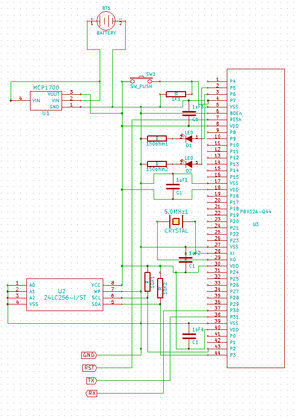
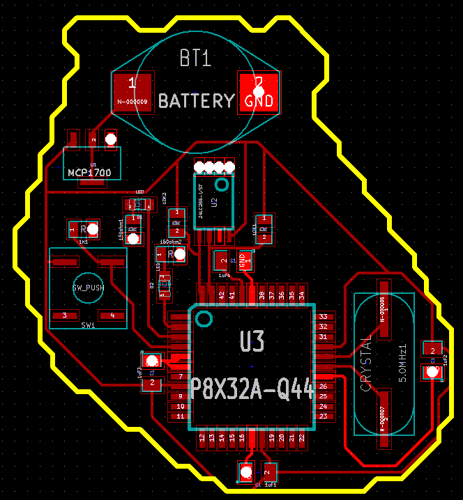
I'm following in Doggiedoc's footsteps in terms of requesting help on my PCB that I've been working on for the past couple of years (heart led project). I now have some vacation time to hopefully bring it closer to completion and was wondering if anyone would be willing to help check to see that the design's sound?
In advance, I know the traces are a major cluster. I haven't been able to figure out a better way of doing it . I'm mostly looking to see if I can get the connections vetted. Most of the boards I've looked at are four layer, not two layer...


If any one has any questions - please do not hesitate to ask! Thanks so much.
PS. Things I have not yet added - the programming pads for the prop plug, and the ground plane (the green gets to me ).
).
Addie
In advance, I know the traces are a major cluster. I haven't been able to figure out a better way of doing it


If any one has any questions - please do not hesitate to ask! Thanks so much.
PS. Things I have not yet added - the programming pads for the prop plug, and the ground plane (the green gets to me
Addie


Comments
- scl and sda are going to pins 43 and 44 (P2, P3) respectively. They should be going to 35 and 36 (P28, P29)
- RESn needs a pullup resistor to Vcc, and to be connected to the programming pads when you get to that point
- You may want to add a 1uF capacitor to the input of the regulator and possibly to the output, although the 4 around the prop should be enough
Someone with sharper eyes and more time may find something else, but that's impressive work for a first board.
Select so bottom plane is connected to GND and everytime a pin needs gnd, put a via there.
Top layer is Power (or Vcc in this case), something needs 3.3v just right click that pin a and select that it should connect to Net named Vcc.
You should not run long lengts of gnd traces on top layers, use two via's instead.
This way you can move the right 0.1uF cap to the left-top of crystal.
You can see that in my attaced Prop Pic, but due to such small space there is no power plane but power-tree-traces.
1. Connect the 4 VDD pins of the prop together under the chip on the top side. The internal connections between these pins is a bit weak so short external connections are recommended. The 4 VSS pins likewise but that is taken care of by the nice ground plane.
2. Pin 7 of the EEPROM should be connected to ground.
3. A ground via should be placed on Prop pins 27, 38 close in.
4. Move the cap from the right side of the crystal to the space between pins 33, 34 and add a ground via.
5. Add a cap and ground via to pin 8 of the EEPROM.
6. The MCP1700 recommends using 1uF caps close to both the input and output pins even with the battery close by.
Lastly, since this board is going to be naked, layout the foils in an artistic way. Possibly to represent the divisions for the four quadrants of the heart.
Have fun!!
Duane J
I'll add the caps for the power regulator.
Kicad's not letting me put a via on pin 7 of the eeprom (but I'll see if i can figure out why).
I knew there was a reason I had originally put the SCL/SDA on 35 and 36. I moved them yesterday to try to expose 37 and 38 for the prop plug, but I guess I'll have to put it back
Thanks for the tip on the via for the decoupling cap on that right side. I knew it was a lot farther away than it should have been, but didn't think to use vias.
And then in terms of the cap and ground via to pin 8 - a decoupling cap? and what would be a good value?
Lookin' cool BTW.
Paul
BTW, what does this board do? I assume it blinks the 2 LEDs as a Thub Lub heart pattern. Anything else?
Are you making 1 unit or a hundred? If a hundred I suggest Bare Board Group, BBG.
Duane J
You probably don't have the space to put one. KiCad prevents you from placing vias (and traces) where it would conflict with minimum clearance.
I tried to get them situated as close to the SA and the AV node (where the electrical impulses initiate from) as I could, but I will probably move them a little once I get to finishing it. The code is even accurate timing wise (as accurate as you can get in spin anyway).
Look okay so far?
I don't see a prop-plug header and also pin7 (RESn) is not connected to anything
It does have internal 5K pull-up as BOEn is set low, but if you are doing any onboard programming it needs to be connected.
And if you only plan to blink LEDs, is a external crystal and 80mhz really necessary?
You should check your beard edge clearance, especially on the top right. It looks like a trace is right on the edge, and so it's liable to be routed off. Also on the bottom near C1.
Your silkscreen looks too small. I find that 35mil width and height, and thickness of 5 mil is good for SMD. You can set it globally by Edit->Reset Module Field Sizes. Any smaller, and it doesn't turn out well.
You should also move component designators out from under the components, so that you can see them when it's installed.
You should add a programming header so that you can load the EEPROM...
What is the little square on the capacitor corners? If it's a polarity marker, it's too small. And if it is, then you don't need to use polarized capacitors (which are more easy to make placement mistakes with).
You may want to add a pullup(down?) resistor on the reset line so that it's not just floating around when there isn't a prop plug.
On the schematic, it looks like you have the resistor annotation backwards: You have the value where the number goes (R1, R2, etc.). Same with the capacitors.
What do you guys think? Just use the internal clock - nix the crystal? (And technically a prop is probably WAY too overpowered for this app)
It wouldn't matter for the Prop plug as far as space is concerned, since the through holes take up just as much space on the back as the front.
I'd keep the crystal pads. You can build a board without the crystal and see what happens, and if you don't need it then you don't populate it. You could also just try it out with a development board now.
C1 & C2 are supposed to be bypass caps, probably with pins 1 grounded using vias to the ground plane.
Not series capacitors.
As far as the PropPlug:
1. In the area between the Prop and the battery you could place 4 holes on 1/10th" canters.
2. You can stick a 4 pin header between the PropPlug and the 4 holes. Don't Solder the Header.
3. Add 3 10K pullups for RESn, P30, & P31.
When done programming just pull out the header.
Duane J
And then in terms of the traces being close to the edge - yeah I will change that once I'm sure that I have all of the components I need and once they're in their general resting area.
And Duane - I'm currently changing the caps. I should've read the datasheet before putting those in.
Thanks for the patience and advice!
Made the caps bypass caps, not series caps
Have you seen this pdf?
http://alternatezone.com/electronics/files/PCBDesignTutorialRevA.pdf
Here are just a few comments...
Since you are using battery power, you should use superbright leds. This way you can use much higher series resistors on the leds - I usually use 3k3-10k, but mostly 10k. RESn does not necessarily require a pullup. Neither does SCL although I always fit it. The pulldown on the pb switch would be better at 10K (usually we do a pullup and switch to ground mainly due to old habits with old chips). If you do not need an accurate clock, then go without the xtal. But would be better to leave provision if you have space.
Use 0.1uF (100nF) accross the prop power/gnd pins and 24LC256 (we mostly fit 24C512 because there is little difference). If your code is small and trying to make it cheaper, then you can use 24C64 but you will need a special loader - I posted one in a thread about this. SInce you are using a battery, you will not have noise so you can get away without proper filtering of the supply. However, it is still advisable to have a 1uF-10uF on each side of the regulator. This will filter out power spikes from the prop switching although your circuit is not going to generate much as it is very basic.
Tx & Rx do not necessarily require 10K pullups. If space is an issue, you can use 1206 quad pack resistors. Extend the pads 0.5-1.0mm out both sides (makes it easier to solder by hand). After a little practice I find it easier to solder these than individual 0805 resistors - easier to keep them steady while spot soldering a pin. Make sure you use a flux pen, and have solder wick for when you place too much solder and need to remove some from a short. Use fine solder - leaded is easiest - I am still here at 60 and have been soldering since 12.
When drawing schematics, it is better in the case you have here to put a straight parallel set of vertical lines for 3v3 and gnd. This makes the schematic easier to read. These would be best placed next to your prop pins or just outside the xtal.
And yes, you could have done this with a cheaper micro, but this way you learn the prop which can be used for many things other chips cannot do.
Others have said, make all connections for prop Vss on one side under the chip, and Vdd on the other. You should also place a separate ground plane around/under the xtal connected straight to the Vss pin beside the xtal pins on the prop. This prevents noise getting into other circuits on the pcb.
If you really want to make a tiny pcb, consider putting components on both sides of the pcb. I put the caps for the prop under the prop on the other side. This increases cost for professionaly assembled pcbs btw.
Here is a pcb of mine that may give you a few ideas..
On the underside are an MCP1702 regulator, 24C512, caps under the prop, transistor circuit for the RESn pin (in case you use a cheaper USB/serial rather than a propplug). This is a 1" sq pcb. The propplug connects to the RHS top pins down (GND,RES,P31,P30). Note the separate gnd plane under the xtal. This pcb is overclocked to 104MHz (6.5MHz xtal).
- You can take away the bottom trace on the left by moving C1 to the other side of the trace, then running (on the top) a trace between the upper left corner of the Propeller.
- You should also put a polarity indicator for the LEDS.
- Personally, I don't like to use via in pad: it might make soldering more difficult.
- Also, you have vias that don't connect to anything. I assume this is to connect to a ground plane: make sure that you define this! It's not currently defined on either layer.
I will be using superbright LEDs. Though the Tymkrs IRC is currently in contention about whether my 3.3v will be enough to run those LEDs. I'll get back to you on that (it'll be on the list)
I'll change the 1k to 10k for the pulldown resistor on the switch.
"Use 0.1uF (100nF) accross the prop power/gnd pins" - I checked the schematics for the PropBoe as a resource, and they used 1uF. Is there a functional difference between 0.1uF and 1uF for these decoupling caps?
The undefined VIAs are for the propplug header that Duane suggested. I still have to get them distanced accurately
And I'd love to be able to use all of the unused pins, but I was trying to design this to maximize battery life - otherwise I totally would have done the whole electrical pathway deal
FF
I've added the ground plane and the power planes. I've gotten rid of redundant power traces, but kept the basics. I've moved the vias out from under the GND pads. I've implemented the header and I've gotten the propplug traces set up.
What do you guys think? I welcome changes!
And for the progression: http://tymkrs.com/forum/viewtopic.php?pid=1238#p1238 - this post on down shows what I changed and why.
And then just highlite the power net to make sure the pour reached every pad.
And the left through-pin don't need a via, as by itself it's a large via.
And extra via deleted! Thanks!
I like to keep the traces in place, just so that I know that there is a possible path for each connection.
The only thing that I would change is to take the two traces off the bottom layer, since you can route them easily enough on the top. But that's a personal preference.
Hmm. How would you do them? Go between C6's pads...under the switch....(it's like a game of snake). And for the ground, I'm also not sure how you would do that.
Actually that is a good analogy, and the autorouter function is a self playing game of snake, some versions faster and more optimal than others.
Frank