

Creating high speed PWM using multiple pins
 Bean
Posts: 8,129
Bean
Posts: 8,129
Here is a program I've been working on. Thought you guys would find it interesting.
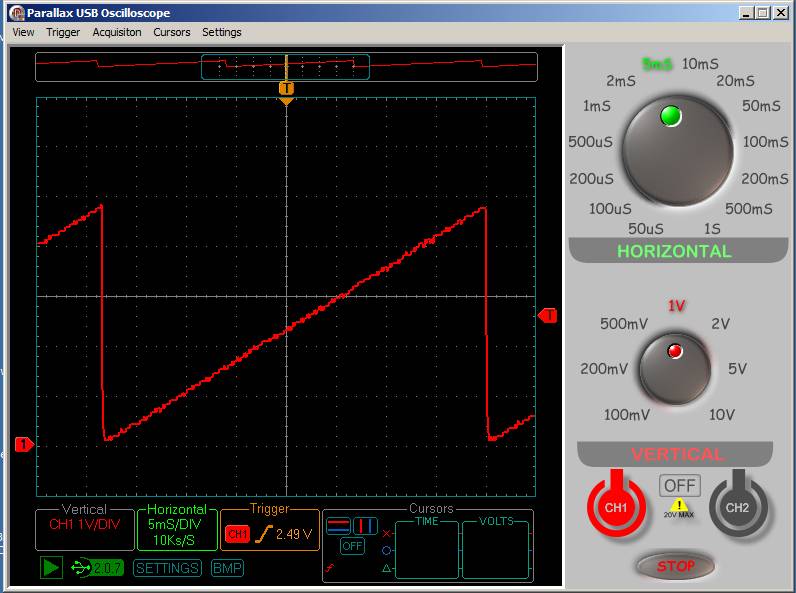
I'll post an oscope picture as soon at I get back home.
EDIT: corrected pdf

Bean.
·
▔▔▔▔▔▔▔▔▔▔▔▔▔▔▔▔▔▔▔▔▔▔▔▔
- - - - - - - - - - - - - - - - - - - - - - - - - - - - - - -
The needy are many, the deserving are few.
Post Edited (Bean (Hitt Consulting)) : 7/10/2009 6:53:51 PM GMT
I'll post an oscope picture as soon at I get back home.
EDIT: corrected pdf
Bean.
·
▔▔▔▔▔▔▔▔▔▔▔▔▔▔▔▔▔▔▔▔▔▔▔▔
- - - - - - - - - - - - - - - - - - - - - - - - - - - - - - -
The needy are many, the deserving are few.
Post Edited (Bean (Hitt Consulting)) : 7/10/2009 6:53:51 PM GMT

Comments
Cool idea. However, I think it's easier do than you think it is.
Imagine that you have a theoretical 3 bit DAC, but treat it as a DAC that can only output up to the highest binary value. This would mean from %000 to %100. Now, imagine that you simply wanted to double the output range of this DAC using your method. We want to turn 0-4 into 0-8. Divide 8 by 4 and you get 2. Now suppose you want to generate the value for 7. Well, 7/2 = 3.5, thus we toggle equally between 3 (%011) and 4 (%100). All other values follow suit, e.g. 5/2 = 2.5, so toggle between 2 and 3.
Now lets increase the output range further. Lets turn 0-4 into 0-16. 16/4 = 4, so there are 4 in between steps, so our PWM rate is now 4X. To output 15, do 15/4 = 3.75. We need to toggle between 3 and 4, only we output the value 4 three times and 3 once. To output 14, we have 14 / 4 = 3.5. This means output 3 twice and 4 twice. 13 /4 = 3.25, so output 13 three times and 14 once. 12 / 4 = 3, so simply output 3 all four times.
This approach will scale up to your 256 levels just fine. The key is to "throw away" some of the DAC's potential resolution in favor of making the math simple. Remember, even though we talk about 8 bit DACs having 256 levels, zero is a legitimate value and thus the top end is 255, not 256. By treating the DAC as if it has a top value equal to the highest binary power, we get to do simple bit shift division, yet still get all the output values we want.
I think you can also simplify this in that the pattern will repeat itself for all the values in between any two real numbers. In other words, for our 0-16 output level DAC (which can be capped at 0-15 via software if you want), we found the following pattern for the values 12 - 15:
15 = 4 (3X) and 3 (1X)
14 = 4 (2X) and 3 (2X)
13 = 4 (1X) and 3 (3X)
12 = 4 (4X) and 3 (0X)
Now lets look at the pattern for 8 - 11
11 = 3 (3X) and 2 (1X)
10 = 3 (2X) and 2 (2X)
09 = 3 (1X) and 2 (3X)
08 = 3 (4X) and 2 (0X)
It's identical, except instead of toggling between 4 and 3, we toggle between 3 and 2. This pattern will continue all the way to the bottom. In other words, you can make a simple lookup table for the inbetween values and it applies to any two actual DAC numbers.
Thanks,
PeterM
I believe a similar concept is used in power inverter designs. See Figure 4 ...
www.tmeic-ge.com/upload/library_docs/english/Drive_Time_-_PWM_1142534311.htm
▔▔▔▔▔▔▔▔▔▔▔▔▔▔▔▔▔▔▔▔▔▔▔▔
Beau Schwabe
IC Layout Engineer
Parallax, Inc.
If your purpose is to generate a PWM sourced analog output, then why not use the "pulse density" modulation approach.·Unfortunately I do not know the name of this algorithm, but·it only needs interrupts at the update rate, regardless of the value to be generated. On top of that the code is consistently just 6 instructions (always) and is bordering on trivial. No thinking to do whatsoever. Assembler of course, but trivial to create a function (or SX/B command for that matter).
The process is to continually add the desired DAC value to an accumulator, and set/clear the output bit depending on wheter the carry was set/cleared respectively:
DAC:··
··················· mov···· w,DACValue······ (of course could be a constant)
··················· add····· DACAccum,w
··················· sc
··················· clrb····· PortBit
··················· snc
··················· setb···· PortBit
Simple as pie...... I use this a lot.
Cheers,
Peter (pjv)
The accumulator approach doesn't solve the problem Bean was trying to solve. He wants to reduce the oversampling needed to have create 8 bit resolution output. With normal PWM or the accumulator approach, if you want 256 levels of output, you need to run at 256 times your desired maximum output clock. His approach is to increase the number of pins while decreasing the oversample rate.
Beau,
Your reference is to how to vary the frequency of a three phase AC motor, hence the three outputs. It isn't related to Beans desire to generate a single output at "high" resolution with a low oversample rate.
Thanks,
PeterM
I was referring to the three-Level PWM waveform in Figure 4. In this sense, by creating different voltage levels, the PWM does not have to span the full voltage range, and therefore can devote more processor overhead to the generated PWM signal effectively giving you more voltage or PWM resolution per voltage level.
▔▔▔▔▔▔▔▔▔▔▔▔▔▔▔▔▔▔▔▔▔▔▔▔
Beau Schwabe
IC Layout Engineer
Parallax, Inc.
What am I not getting here..... the accumulator approach gives 256 levels of output, all with negligible overhead, and does so in the ISR as a "background task".
Cheers,
Peter (pjv)
For example,
to output a sinewave in 32 8bit DAC-values:
The accumulator approach requires 32*256 interrupt cycles to complete.
If you were to use 8 pins and a R-2R ladder network, then all you need
is mov port,variable to set a DAC value, and the sinewave will be
completed in just 32 interrupt cycles, so you will have a higher frequency
output.
regards peter
Here's the relevant part of Bean's PDf file:
Thanks,
PeterM
You're correct about the area involving figure 4 not being simply about 3 phase motors. However, my reading of the article section you pointed out leads me to believe they are doing a vaguely similar thing with a very different idea in mind. In Bean's case, he specifically wants to reduce the interrupt rate while retaining full 8 bit resolution. In the AC motor case, it appears they simply want to have some crazy high power/high voltage motors controlled by independent PWMs that are added together to create the illusion (to the motor) of a single monster PWM. In the article it says:
For example, the three-level inverter in Figure 4 has two independent 2-level inverters arranged so that the output voltages add.
They are talking about motors running at 2400 and 4160 volts. Yikes!
The article doesn't clearly point out why they want to use multiple independent PWM sub-systems. I'm not sure if it's a problem to create a single high power PWM at those voltages. However, they aren't talking in the article about faking a high resolution ADC and lowering the interrupt time for the CPU. Perhaps they want a lower interrupt frequency to better deliver power to the motor? I know that tailoring PWM frequency to the load can help make for a more efficient transfer of power.
Thanks,
PeterM
Instead of dividing my 37 (instead of 32) another method of implementation is to have a second LSB bit (so a forth pin with a 4K resistor). In this method, after setting the 3-bit DAC with (Value / 32)This "second LSB" pin is then the only pin toggled just like standard single pin PWM (with value // 32 * 8) . Of course this requires 1 more pin and another resistor.
Bean.
▔▔▔▔▔▔▔▔▔▔▔▔▔▔▔▔▔▔▔▔▔▔▔▔
- - - - - - - - - - - - - - - - - - - - - - - - - - - - - - -
The needy are many, the deserving are few.
Post Edited (Bean (Hitt Consulting)) : 7/11/2009 1:31:07 PM GMT