

Wiznet W6300
 ke4pjw
Posts: 1,312
ke4pjw
Posts: 1,312
Working code can be found here:
https://griswoldfx.visualstudio.com/_git/Spinner Edge II
Looks like Wiznet just dropped the W6300.
https://docs.wiznet.io/Product/iEthernet/W6300/overview
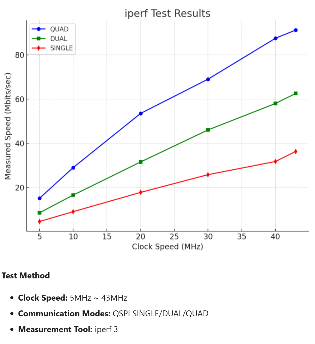
I hope this solves one of the problems that I found with the W6100. That is that UDP, when drinking from the firehose, would overrun the buffer. You literally could not get data out of the chip fast enough to keep up with the type of data needed for my light controller project. This chip has quad SPI and a 32K RX buffer.
I will be experimenting with it and the P2 as soon as I can get my hands on hardware. I will keep you all posted. The datasheet's registers are very similar to the W6100, so I am hoping the lift won't be too much.
--Terry
Comments
Quad SPI, and QPI, via smartpins needs some acrobatics. Placing the clock pin in the middle of the data pins is a must, so then it can be routed to all four smartpinB inputs.
The down side of doing that is it then precludes the streamer as an option since that requires the data output pins to be consecutively ordered.
So you basically have to choose up front if you want to invest in the performance of DMA'd streamer ops, or stick with managing four serial shifters while massaging the data back and forth between serial and parallel.
EDIT: On the other hand, it wouldn't be a big deal to include a few jumpers to the board layout to allow reordering of the clock and data pins. That would allow both code paths to be explored without needing two board designs.
Hope this helps the planning at least.
@ke4pjw Didn't your board use the 8-bit bus? That has to be fastest interface, right?
Just got some w6100io modules to hopefully enable the ethernet port on the PLC thing working on.
No sign of w6300io yet though...
Just plain SPI for me. Does bigger buffers help in that case? Guessing not, but can't hurt.
My board does both. SPI is only on one of the 12pin connectors and it is on the one that needs power. If you wire the io board up, my driver would work with it as it supports both parallel and SPI. Also, my driver is cogless, unless you are reading E1.31 data.
I never could get the speed fast enough in SPI mode for 40fps @ thousands pixels.
My only complaint about the W6100 is the poor UDP performance at 100mbps.
--Terry
I requested one of the W6300 samples from WizNet and they reached out via email today. I may have one in hand, later this month.
--Terry
So I have started on the Spinner Edge II with the W6300. Wiznet sent me some samples. I have a couple of the raw ICs and I also have 2 of their RP-2350 based boards. (Too bad I can't figure out what tools are needed to program them)
I will only implement QSPI on the SE II, as that is what they recommend for best performance. (I really want that 90Mbps)
Below is my (only checked over once) schematic. @evanh take a gander at the Quad SPI frame format. Is that unusual? Should I choose better CS and CLK pins? I think it would be helpful to have the nibble on a valid boundary to shift out data. I am not sure how or if those bit twiddling gymnastics could be performed by a smartpin.
Please feel free to throw rocks. If there is going to be a problem, I want to know about it up front.
Given that the instruction phase is sending 8 bits on QD0 with QD1-QD3 as don't care you can still make use of the streamer to send it all out in a contiguous block. You just need to distribute the 8 "I" bits into the streamed command - the MERGE instruction would let you group 8 bit instruction into nibbles and send it out with the LSB sending the data (although you'd need to reverse the 8 bits beforehand to send MSbit first, unless you setup the streamer to do the reordering). You'd first stream the instruction then the 16 bit address and 8 bit dummy and the real write data for writes, or for reads turn the bus around to read it back during the dummy step. Timing is everything but it's all doable. You need the nibble aligned on a 4 pin boundary if you use the streamer for highest performance. Other control pins can be anything. The clock would be generated by a smart pin and be some multiple of the P2 clock period. A 200MHz P2 could read up 100MB/s for example, although you can do it slower at 12.5MB/s and that still supports 100Mbps transfers.
Well, I guess I need to get a few of these built so I a can start poking at it.
The boards and all the parts have arrived. Hopefully I will have some time tomorrow night to make a couple of them. If anyone is interested in helping me develop a driver, PM me.
Well, it's real. It gets link and activity, so I can assume the oscillator is running. I can also pull P7 low and it will reset. (Loses link and comes back when expected)
Now I need to figure out how to do more than poke it with the proverbial stick")
Oh, also, the V1.0 datasheet was wrong. They had pin 10 as 3v3A. This did not match their example boards. I raised the issue in email, online forum, etc, with no response. I checked yesterday, and the V1.0.1 datasheet was created on the day I reported the problem. Glad I went with their example in my layout and not the datasheet.
It appears that I should be able to communicate with this chip using straight SPI. The command phase is what determines the SPI mode, which is why it always starts off in standard SPI. So far no luck. Time to put a scope on it.
Looks good. Hope you can get it talking…
Well, when I scope probe QD1, I do see data, but the SPI driver isn't returning data. I am going to throw the logic analyzer at this and see what's really going on with all of the pins. Based on the datasheet, I should send 3 bytes, all zeros, for it to be set to pull the chip version number, then read a dummy frame, and then I should get valid data.
Instruction byte:
bit 7-6 : 00 is single SPI mode
bit 5 : 0 Read Access
bit 4-0: 000_00 Common Register (Where the chip version lives)
Address bytes:
$0000 - This should be the address of CIDR0, the major ChipID.
Read phase:
Clock a dummy read byte.
Clock a byte to get $0000 value (Expecting 00)
Clock a byte to get $0001 value, (Expecting 61)
All I get are $00 on the P2. Running the SPI in mode 0, which is valid for this chip.
Maybe there are mode pins you need to set for regular SPI mode?
My reading of the datasheet is the there are two mode addressed by hardware. Either parallel or QSPI. When in QSPI mode, you can set the SPI mode as a part of the instruction byte. I do not see any data being clocked out on the other two DO lines, just D1 as expected when you set the mode as 00. (Single SPI mode)
Sorry, I didn't see your request for help. The pin order you've chosen for 4-bit wide suits the streamer, not smartpins. I would have recommend using the streamer for 4-bit anyway. It is a little tricky but you get benefits for the effort. But we'll get to that after having success with 1-bit SPI mode first.
Okay, 1-bit SPI operations:
Operating smartpin P_SYNC_TX mode (%11100) has it's sequencing tricks. Start-stop and continuous update modes have a subtle difference in initiating. In continuous mode, X[5] = 0, if you raise DIR before loading Y with the data then it will send all zeros for the first word. Whereas in start-stop mode, X[5] = 1, it works entirely on clocks for buffering, DIR is ignored I think.
Another area to pay attention to is clocking a tx smartpin for sync serial. If you're working with a small clock divider - usually the case - then the Prop2's I/O staging latencies will need to be compensated for. It differs depending on the divider value in use. In the clock smartpin setup, either P_PULSE (%00100) or P_TRANSITION (%00101), what WXPIN value are you using for the divider right now?
Rx sync serial smartpin mode, P_SYNC_RX (%11101), should be the easy part. It doesn't have to worry about I/O staging latencies since the incoming clock and data signals follow matching paths. Set the word length is about it. Then just have to look for IN high and use RDPIN to clear the buffer, returning IN low.
EDIT: Oops, it's worse than I thought! The tx smartpin, in P_SYNC_TX mode, can't be internally routed for the clock pin. The two pins are too far separated at the Prop2. Unless you're into cutting tracks and pin jumpering, you're locked into doing streamer ops straight off the bat I'm afraid.
PS: A pin order that could have done both streamer and 1-bit SPI would be:
That places CLK pin right next to QD0 and QD1 to assist smartpin routing, and it keeps the data pins in order on a 4-bit boundary to suit the streamer.
So, it looks like this was a hardware problem. The 1.2V had a low resistance on C4 and was causing the Wiznet to fold back and reboot. I am guessing this was solder that didn't fully melt or some debris made it's way under that component. It was showing shorted to ground. Luckily I only had to remove two caps to find the problem. Swapped out the Wiznet just to ensure it wasn't damaged. Now I can read what I expected!! W00T! Spent way too much time on something stupid. I want one of those PickSoEasy PSE-3000's. This stuff is microscopic!
@evanh I guess I didn't understand before about the clock being on an adjacent pin to the data. It's not the first expensive mistake I have made") I must admit that I really don't understand either the streamer or the various smartpin configurations. I didn't think it could be used to clock in nibbles. Currently I am using Jon's bit bang SPI driver (jm_spi.spin2).
I must admit that I really don't understand either the streamer or the various smartpin configurations. I didn't think it could be used to clock in nibbles. Currently I am using Jon's bit bang SPI driver (jm_spi.spin2).
I will review the various smartpin configurations to understand what I should do for the next iteration of the board. I might be able to easily bodge the trace for my own use. Your idea of jumpers was a good one. I appreciate your suggestions!
Hehe, layout and assembly issues always seem a little on the damn-it side of things. Good to see you solved it in less than a day really.
And those tiny components are a horror to find again if they get accidentally shaken or flicked off the board.
I can provide example source code for using the streamer when it comes time. You'll appreciate the direct to memory results.
Probably no need to spin a new board if the streamer can be used instead which should be possible if the clock rate is just some integer division of the P2 clock, although for a generated clock you'll still use smartpin modes for that pin. At low speeds like 25MHz the timing should be simple to meet unless the P2 is being clocked really slow as well. It does complicate the code a little initially to sequence the different transfer portions, but it'll still do the job. You can even do other things while you wait until the transfer is complete.
Managing four data smartpins isn't fun anyway. It's a fiddle reading and writing them all together combined with the mashing of bits to go between serial and parallel formats. Quad SPI is in reality a parallel data bus.
Keep using Jon's SPI code until you're ready to make the jump to streamer ops.
What is the bus speed here? Looks to me like might be around 25 MHz.
Do you really need the streamer for that low a speed?
Native 1-bit SPI at 100 MHz isn't possible because, due to I/O staging latencies, sysclock/4 is smallest clock divider a tx smartpin can be operated at.
My pinout list above would also work for Dual SPI using serial smartpins - Which should be manageable at 50 MHz SPI clock rate. The resulting code size would also be smaller than any Quad SPI solution.
A Quad SPI solution using serial smartpins would need the CLK pin wired between data pins on the Prop2. eg:
This pinout would not be compatible with the streamer.
According to the chart above, at 25MHz, overall throughput is greater than 60Mbps using quad SPI. That should achieve the kind of performance I am hoping for.
Streamer would have no issue hitting 50 MHz if you wanted to.
@evanh Can you "fire and forget" the streamer for x numbers of bytes?
Yes, but it uses the FIFO so you have to stay in Cogexec for the duration of the transfer. Which kind of means staying inside the ORG/END code section. More specifically, not using Hubexec nor Xbyte nor any explicit FIFO instructions until the Streamer has finished its transfer.
Flexspin compiles to native Hubexec. Pnut uses Xbyte I think.
PS: The SD card driver uses that time to generate CRC of the transmitting data block, or check CRC of prior data block received.
We have success. Only a couple of lines (literally) changed in the W6100 driver to make it work.
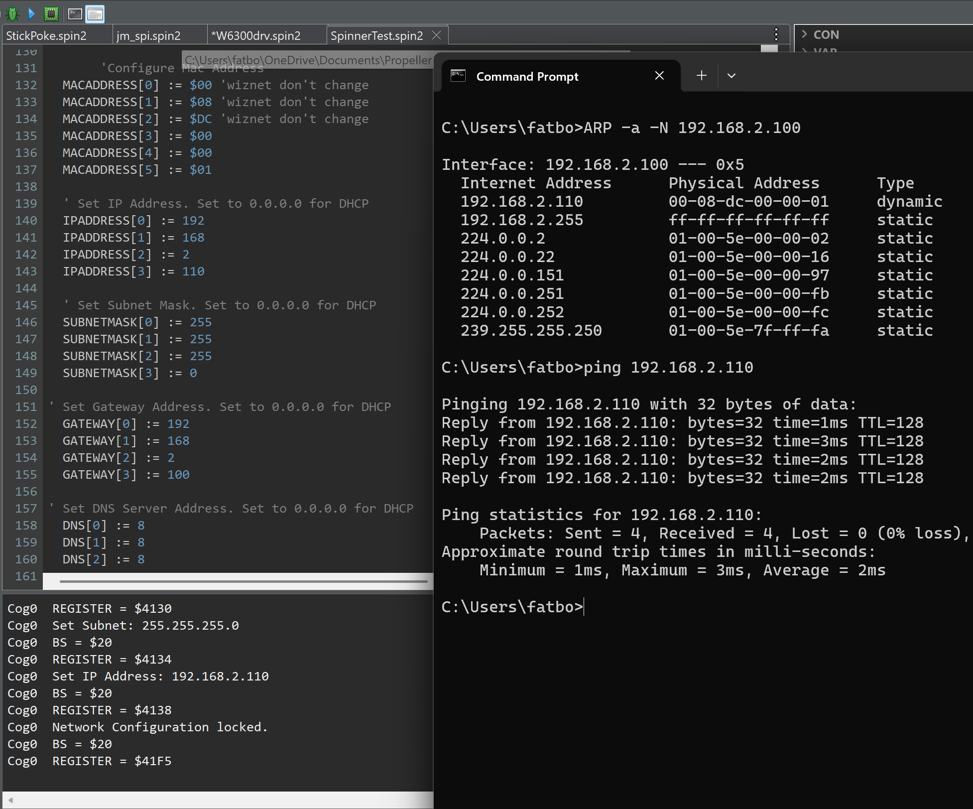
Spoke a little too soon. I can talk to the common registers. I can create a listener, but the data that is transmitted is all corrupt. Close!
Ok, this has to do with the constants that had to be changed for the block selection. Probably a few more touchpoints to update the methods that access the read/write buffers.