I ran the memory test with just the fan blowing on the top surface of the P2 and while it failed the memory test after just a minute or so, it let me play the MSlug game for at least 15mins before I stopped playing. So having memory test failures early doesn't necessarily correlate with game lockups, although I didn't run it for an extended time. Ambient room temp is 22C. I probed the edge of the P2 and saw about 38C but this is not the hottest part.
If I do make another variant I think I could put the P2 on the top surface of my FireAnt P2 board with a single sided load. When I measured the inside of the case this leaves about 6mm from the PCB top to the inner top edge of the cartridge. A 1.2mm P2, a 1.5mm AL plate and a 3mm fan would just fit. The fan would sit over the P2 and blow air down onto the plastic case. Cuts in the AL plate would allow some airflow around the hot areas. Holes may need to be drilled above the fan in the case for intake/exhaust.
The only other way is to somehow route out the plastic case underneath the PCB for the P2 to sit exposing the ground on the top surface but it makes assembling the board very difficult with a double sided load, and I'm kind of wondering where all those bypass caps would go too. I'm still deliberating...
@Rayman said:
Would it run at 300 MHz with no special cooling?
I suspect it would depend on how active the Cogs are. If they are not all at 100% active on all peripherals it may potentially be achievable but can't tell for sure.
I'm thinking that some of this might be related to the PSRAMs getting hot and performing worse at high speeds. My board doesn't have a great path to PSRAMs vs the P2 Edge for example. Some IO has to snake around on Lachlan's board to reach the mezz connector to reach my own board's layout and despite fitting the 32MB at the far end of the bus to avoid an extra stub hanging off the end to generate reflections etc, it has some traces than hop from layer to layer and no impedance is controlled. I noticed this in my initial delay test results. The timing windows of operation already rapidly taper off close to the 338 MHz operation at room temp, and increasing the temp probably makes it worse by heating some chips differently to others. 300MHz may be safer. I wonder if these games can still work at that rate in a test, just that the pitches are off and the screen is refreshed slower - may try that out...EDIT: actually probably simpler to just run the RAM test at 300MHz..
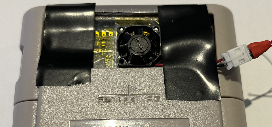
I ran the RAMtest slower just by setting CLK_MULTIPLIER to 12 instead of 14 (~290MHz), and it has already lasted over 15mins with no issues, with no fan no heatsink and fully sealed up in my intact case cartridge (not the earlier one with the huge cutout at the back). I'll stop it at 20mins open it up and quickly measure the temp it gets to.
Update: reached 20mins okay and I stopped it there yanking it out and quickly measured the P2 temp. IR thermometer showed a 68C peak and then was seen reducing after that as it cooled down. 20C ambient. So even though the P2 was as hot or hotter than in the earlier failures, the RAM was still good at this frequency...interesting.
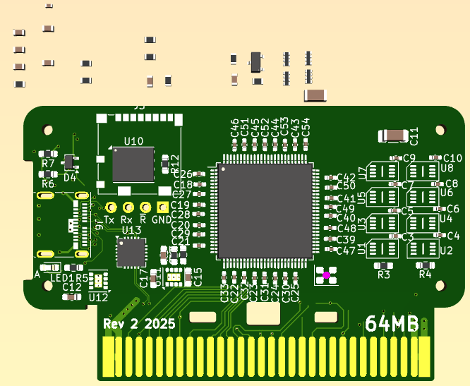
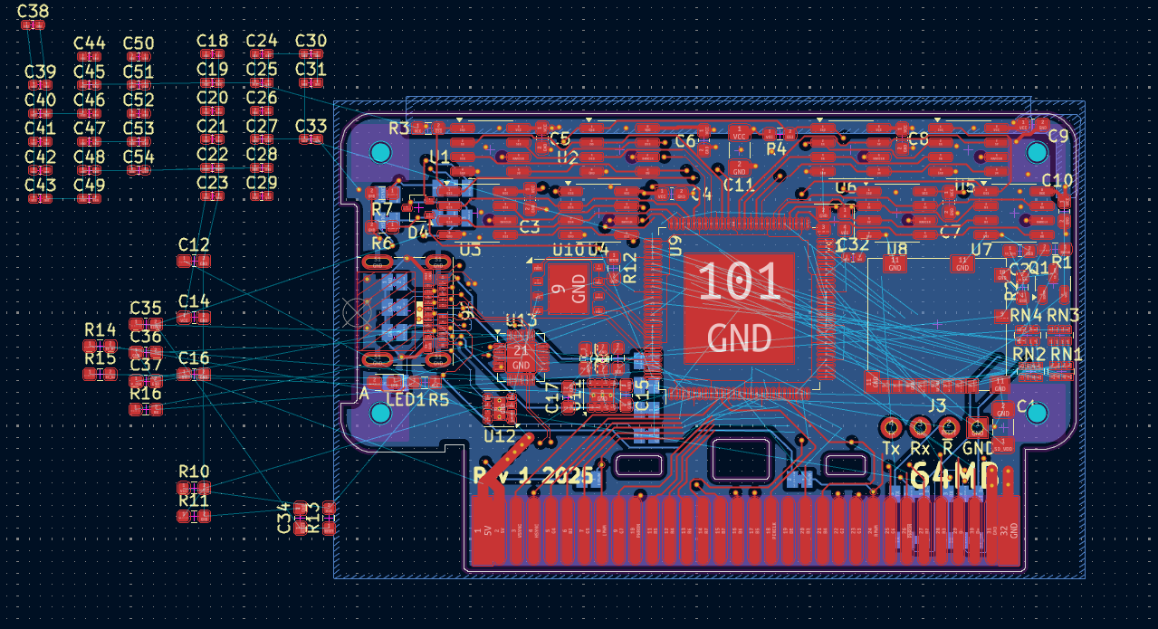
I do wonder if I layed out a new FireAnt P2 variant on a single PCB if the memory traces could be tidied up whether we'd get a better result even up at 338MHz. Maybe kill the 64MB option to eliminate any intermediate pad RF stubs with the second unpopulated bank. There are also probably ideal ways to design it to correctly terminate the data bus for best impedance matching, but I'm no expert at that sort of stuff. I did put a series resistor on the clock line which could be tweaked. Would need a decent high speed scope to see the benefits and for tuning and I don't have access to that right now. On a new board it wouldn't be a 0402 either, making it simpler to alter.
UPDATE2: Also just ran that RAM test for 20mins fully enclosed with no cooling at a CLK_MULTIPLIER of 13 (314MHz) and it passed the RAMtest there too. I'd kind of expect equilibrium to be reached by then at this load but it may still be rising slowly - ideally I need to try to feed a thermocouple in there to see when exactly it tops out. P2 temp got up to 77C (wow it's cooking), room temp was 20C. What happens if the P2 gets too hot????
@Tubular said:
Hmm does it look more possible if the P2 is rotated 45 degrees?
You can place 0402's on as close as a 0.94mm pitch and still have compliant courtyards, apparently.
Maybe if I move the RAM bus around by 8 pins it might or perhaps move all 4 RAMs to one side. I know with the P2 installed on the back side it would free up space for bypass caps (with boatloads of vias), or even try to put the bypass caps on the back with manual soldering. But a single sided load is more appealing to try to make with my hotplate. I'm really starting to think the RAMs are mostly just failing "early" (LOL they are overclocked to begin with) due to temp rises in the case. With a small internal fan sitting on the P2's TQFP's plastic side and tighter PSRAM routing I'm still hopeful it could work. We are already fairly close if it already sustains good reads for 20 mins at 314MHz and even hits 77C without failing/lockups. We just need that last 5-10% for more margin.
@Wuerfel_21 said:
If RAMs are running sysclk/3, they're not overclocked.
True. It was sysclk/3 in the test.
RAM test fails can come from a lot of places, which is why they're tricky:
Bad timing
Bad signal integrity (uneven trace length etc - though that should show preference to certain lanes failing)
RAM unhappy somehow
P2 Hub RAM glitch (though IME the RAM test program kills the kinds of boards that have the hub glitch happen immediately at startup)
I think it could be signal integrity being marginal, and that increased temps soon pushes it over the limit. I've not found a better timing setting than what I already used.
One lane (LANE0) does seem to fail before the others in the tests but others follow soon after. Reflections in the clock signal not being diminished at the source perhaps. I star wired it with equal trace lengths for the clock to reach each PSRAM, but not as much for data bus, although they were reasonably close on my board (less so on the P2 board above perhaps). If I can successfully desolder the 0402 in the clock net I could try a small source resistor like 22 - 33ohms or something. Right now it's just a zero ohm resistor.
@Tubular said:
Here's a fan plate I generated today. There's a few different ways to use/mount this, and it takes either a 20x20 or 15x15mm fan
Neat. Would be handy sitting above your P2DU to blow air over the P2, although I guess you lose access to some top pins. Pity the smaller fan doesn't fit inside the 2x6 header gap. Maybe an under mount would still be possible if your board sits up more than 6.2mm from a lower PCB surface giving space for the 5mm fan to blow air around the 1.2mm P2 height. Or smaller if that tiny 3mm fan is used for example. That'd still leave height for clearing your other tallest components like the USB-C connector but you would not have the ability then to mount with solder nuts as they are blocked on that side so you'd probably need a row of though hole pins down each edge to hold it instead.
we faced similar stability issues with PSRAM while designing our "P2 Thing" board.
Ended up with a stable sysclock / 3 96 MB on 3 banks configuration (sysclock @ 334 Mhz).
For some reason sysclock / 2 also works reliably by using only 64 MB and disabling one bank.
If could be of any help what solved our stability issues was
Used smallest available package for RAM ICs (APS6404 package USON-8 2X3). Smaller version is also faster.
Moved RAM chips in the closest possible position with respect to the propeller 2 (see layout image)
6 layer PCB (previus 4). Bottom layer and one inner layer for heat transportion to the exterior using everithing available like connectors etc as heatsink.
In this way P2 runs also at 365 Mhz.
Top layer
Data Bus
Full copper Inner and Bottom layer for heat transportation to the exterior
Heed his words, that design runs very stable despite being in an enclosure with no cooling, not even air vents.
Interesting that the north and west sides of the copper plane are blocked by all those vias...
EDIT of note: I just noticed I have left the MXX Thing running MisoYume (at 343 MHz!) for multiple days while tending to Other EndeavoursTM and it has not crashed. Reliable engineering.
Thanks @MXX. Yes I really like your memory layout - clean consistent traces on each lane. I know Lachlan and I talked about using the USON-8 parts some time back but seemed to be hard to acquire at the time. We can look again for those. It would free up extra space on the board too such that there may be better layout options for the extra PSRAM on the board. A 6 layer board was another option but I think we needed to be at 0.8mm total thickness for the edge connector to fit nicely which limited the design with the manufacturer selected. The originally supplied PCB thickness was something even thinner like 0.7mm.
Still considering what to do but this is really useful input. Moving to USON-8 size is a good challenge to try do by hand but I would be up for it given earlier decent results with fine pitch stuff on the hotplate. Good to try to push the skillset to the next level. Along with using 0402 from 0603 etc.
@Wuerfel_21 said:
EDIT of note: I just noticed I have left the MXX Thing running MisoYume (at 343 MHz!) for multiple days while tending to Other EndeavoursTM and it has not crashed. Reliable engineering.
Looks like Mouser has some USON-8 PSRAMs in stock right now at 3.3V which is good.
However browsing the data sheet I noticed an interesting data point. It seems to say the rated performance is lower for higher voltages. This P2DU board has a higher VCC output of 3.47V IIRC which is potentially reducing performance even more. So I wonder if we drop the IO voltage down a bit whether we might get better PSRAM performance. I also question if this is the correct way around...? Usually it's the higher voltages let you overclock more, so maybe this is some thermal or peak IO slew rate issue from IO current restrictions in the device which reduces performance at higher voltages as it takes longer to fully stabilise between wider logic levels thresholds or something like that. Like how you can drive IO faster if it doesn't change the voltage as much in low voltage differential signalling systems.
Note *: 133MHz for 32 Bytes Wrapped Burst operation at VDD=3.0V+/-10%
109MHz for 32 Bytes Wrapped Burst operation at VDD=3.3V+/-10%
I note also the APS12804 have appeared on Mouser. No stock yet, and only 1v8 available at this stage, but the APS website says these are now in MP so hopefully 3v versions are not too far away
Just wired up a janky way to drop the IO voltage down to lower than 3.46. It's now set for 3.1V but can go lower than this via 2Mohm pot adjust in the feedback path of the 3.3V switching regulator.
Gonna try a few tests to see if this helps the memory performance.
At 3.1V the PSRAM seems to behave slightly differently. Previous results here https://forums.parallax.com/discussion/comment/1570101/#Comment_1570101 and here https://forums.parallax.com/discussion/comment/1570132/#Comment_1570132 tapered later than this but this version transitions to the next 14 clock delay "half-step" up at 341MHz to 350MHz, showing it still working at the higher frequencies....maybe this is actually good result despite less band overlap around 338MHz where we want to operate. The earlier results were fading out at the top end when hot too. Need to test more for some more definitive results with Wuerfel's RAM tests.
I'd say if there's only one good setting during that transition, that one might actually be better, as that'd mean it's sampling the Eye dead on center.
Good to have some proof that VIO affects PSRAM performance. Luckily it shouldn't be hard to design boards to have an extra-low VIO rail for PSRAM pins without affecting the rest of the I/O.
@rogloh
At the time I also tried PSRAM @ exactly 3.0 V to see what happens.
I didn't noticed any improvement (seems worse), don't know if it was due to the lower PSRAM voltage or the P2 IO not working well at that voltage. Cannot find any spec about P2 VIO.
About manually mounting USON-8 size should not be too difficult as they have a central pad that helps alignment.
Could you provide the piece of software used for your tests, please? The one giving the table with different delays. Thanks
@MXX said:
@rogloh
At the time I also tried PSRAM @ exactly 3.0 V to see what happens.
I didn't noticed any improvement (seems worse), don't know if it was due to the lower PSRAM voltage or the P2 IO not working well at that voltage. Cannot find any spec about P2 VIO.
About manually mounting USON-8 size should not be too difficult as they have a central pad that helps alignment.
I agree that so far it does seem a little worse but it hasn't been thoroughly tested yet - it didn't seem to help Wuerfel's RAM test when I tried it today, it still fails almost right away - about a minute or less. I wonder if the signal timing differences related to the lower voltage range or from reflections at different operating frequencies/delays is negatively affecting the sampling eye in this 320-340MHz operating region, but I'd need a decent scope to see that happening while the voltage is changed. Normally the half steps extend the bands and taper off one at a time, but in the case just posted above both adjacent values taper at once. I can only imagine that sort of thing is occurring if the data or clock signal is rather distorted, like overshooting/ringing etc, and not a nice clean signal transition.
Could you provide the piece of software used for your tests, please? The one giving the table with different delays. Thanks
Sure, here's the link to the software I use below. It's in this p2memorydrv.zip file and you want to build the file called psram_delay_test.spin2. It will run at 115200bps over the download serial port and prompts for pins and test range etc. It's setup for 32MB of PSRAM but can be tweaked to test more PSRAM fitted on other banks by just changing the chip select you input. It'd be interesting to compare with your own board to see what you get over the same range from 300-350MHz. I'd imagine it tapers between delay bands nicely vs what I'm seeing on my board.
Also I was going to ask, how are you routing the clock to your devices, is it snaking around as a single trace or do you fan it out from the P2 to each device separately from the source? Your picture seems to show rows of clock nets to each group of 3 PSRAMs per nibble but where are they connected together? Was a little hard to see that.
@Wuerfel_21 said:
I'd say if there's only one good setting during that transition, that one might actually be better, as that'd mean it's sampling the Eye dead on center.
Good to have some proof that VIO affects PSRAM performance. Luckily it shouldn't be hard to design boards to have an extra-low VIO rail for PSRAM pins without affecting the rest of the I/O.
Certainly it's changing things, whether good or bad may be difficult to fully tell yet as I may have other signal issues on my board. A lower VIO rail may also reduce overall power consumption/self heating a small amount too, but PSRAMs don't burn very much power, 5.5mA was quoted at 133MHz for each device, excluding IO load current. This result may also show that large amounts of switching noise on the VIO rail of around 200-300mV or so could really affect performance by shifting the bands around a bit. So if your board is marginal to begin with the extra supply noise could potentially take you from one band to the next. That's a lot of noise though. Make me want to go scope this IO voltage supply now.
From what I understood the driver runs PSRAM chips at sysclock / 2, isn't it?
@Wuerfel_21
at 334 Mhz, like in NeoYume, the delay sweet spot seems to be 12.
In NeoYume config I have to set PSRAM_DELAY = 14.
Are these two delays related somehow? Maybe PSRAM driver is different?
Also I was going to ask, how are you routing the clock to your devices, is it snaking around as a single trace or do you fan it out from the P2 to each device separately from the source? Your picture seems to show rows of clock nets to each group of 3 PSRAMs per nibble but where are they connected together? Was a little hard to see that.
First image shows clocks and CS routing.
Second image is inner layer power supplies.
at 334 Mhz, like in NeoYume, the delay sweet spot seems to be 12.
In NeoYume config I have to set PSRAM_DELAY = 14.
Are these two delays related somehow? Maybe PSRAM driver is different?
Yes, the values are not portable. Roger mixes the sync data setting in with the delay and applies some constant offset.
@MXX said:
From what I understood the driver runs PSRAM chips at sysclock / 2, isn't it?
Yep, the tester producing max of 4 good columns per frequency confirms that. You'd get up to six good columns for sysclock/3.
The good columns for "delay" comes from, at sysclock/2:
A ) there being two possible latency alignments (lag) in raw clock intervals, and
B ) a small delay line effect is introduced via clock pin registration. So the least bit of "delay" controls enabling this registration, aka sync. Basically, this is a convenient hack for fine adjustment.
This is a general streamer <-> smartpin mashing up mechanism that the driver software has to manage. The smartpins run independently of the streamers and cogs so there is a number of steps to get the two aligned. I use the same approach for the fast 4-bit wide SD card driver code too.
Some applications have data pin registration used also but does not improve resolution of lag adjustment. It's either always on or always off.
thanks for the test code, this is what I got on a 32 MB bank on my board
That's such an awesome result no wonder your board is rock solid.
From what I understood the driver runs PSRAM chips at sysclock / 2, isn't it?
Yes data transfers at at half P2 (sys)clock speed, though it will transfer at a data rate of sysclock MBytes/sec for 16 bit PSRAM. Can be confusing at times if these are mixed.
@Wuerfel_21
at 334 Mhz, like in NeoYume, the delay sweet spot seems to be 12.
In NeoYume config I have to set PSRAM_DELAY = 14.
Are these two delays related somehow? Maybe PSRAM driver is different?
Yeah as Ada mentioned my driver is different - I only had a 4 bit field to hold this delay value in the driver so I needed to add an offset to maximize the range. Plus the LSbit of this delay is actually the "half step" of the overall delay - so the full range is only 8 P2 clock cycles worth.
Thanks for the better pics. It looks like you use 1 clock column trace which feeds 4 row traces of with 3 chips(banks) per row or nibble. It's a very tidy arrangement albeit not length matched. Doesn't seem to matter as still gives a damn good result in the test. Well done.
UPDATE: Also I just measured the noise on the VIO rail - am only seeing 70mV p-p max noise or occasional worst case spikes on scope in persist mode so it's probably not that noisy. There are a lot of IO switching pins with the parallel video output but it's all pretty well bypassed on the P2DU board and the 3.3V regulator has a high 3A max output capability.
Had a rough mess about with the PCB placement and it looks more promising to fit on a single board with the smaller PSRAM chips, plus allows for the cleaner routing to the RAMs now on the right side. The uSD card reader is not the correct footprint and is just a placeholder for now; I'd use one of those slim readers with the card sitting inside above the flash chip. EDIT: alternatively I could put it back where it is meant to go facing out the side of the cartridge and move the USB-C to the top facing upwards - that would require an optional cut-out on the top edge for exposing the USB-C for debug/download and/or VGA/component out. Potentially better if you run a USB-C cable outwards towards a TV for example.
Also found that the ENIG 6 layer board is 2x the price to make over the 4 layer one I did last time (~$53 vs $26 AUD or so in 5x qty), but can actually be made in 0.8mm thickness which is good to know.


Comments
Awesome, thanks for confirming that.
Vertical fins it is then... and perhaps a small 20mm fan on AL substrate
I ran the memory test with just the fan blowing on the top surface of the P2 and while it failed the memory test after just a minute or so, it let me play the MSlug game for at least 15mins before I stopped playing. So having memory test failures early doesn't necessarily correlate with game lockups, although I didn't run it for an extended time. Ambient room temp is 22C. I probed the edge of the P2 and saw about 38C but this is not the hottest part.
If I do make another variant I think I could put the P2 on the top surface of my FireAnt P2 board with a single sided load. When I measured the inside of the case this leaves about 6mm from the PCB top to the inner top edge of the cartridge. A 1.2mm P2, a 1.5mm AL plate and a 3mm fan would just fit. The fan would sit over the P2 and blow air down onto the plastic case. Cuts in the AL plate would allow some airflow around the hot areas. Holes may need to be drilled above the fan in the case for intake/exhaust.
The only other way is to somehow route out the plastic case underneath the PCB for the P2 to sit exposing the ground on the top surface but it makes assembling the board very difficult with a double sided load, and I'm kind of wondering where all those bypass caps would go too. I'm still deliberating...
Would it run at 300 MHz with no special cooling?
The thing I made could only really run MegaYume . That’s the easiest, lowest freq one…
I suspect it would depend on how active the Cogs are. If they are not all at 100% active on all peripherals it may potentially be achievable but can't tell for sure.
I'm thinking that some of this might be related to the PSRAMs getting hot and performing worse at high speeds. My board doesn't have a great path to PSRAMs vs the P2 Edge for example. Some IO has to snake around on Lachlan's board to reach the mezz connector to reach my own board's layout and despite fitting the 32MB at the far end of the bus to avoid an extra stub hanging off the end to generate reflections etc, it has some traces than hop from layer to layer and no impedance is controlled. I noticed this in my initial delay test results. The timing windows of operation already rapidly taper off close to the 338 MHz operation at room temp, and increasing the temp probably makes it worse by heating some chips differently to others. 300MHz may be safer. I wonder if these games can still work at that rate in a test, just that the pitches are off and the screen is refreshed slower - may try that out...EDIT: actually probably simpler to just run the RAM test at 300MHz..
I ran the RAMtest slower just by setting CLK_MULTIPLIER to 12 instead of 14 (~290MHz), and it has already lasted over 15mins with no issues, with no fan no heatsink and fully sealed up in my intact case cartridge (not the earlier one with the huge cutout at the back). I'll stop it at 20mins open it up and quickly measure the temp it gets to.
Update: reached 20mins okay and I stopped it there yanking it out and quickly measured the P2 temp. IR thermometer showed a 68C peak and then was seen reducing after that as it cooled down. 20C ambient. So even though the P2 was as hot or hotter than in the earlier failures, the RAM was still good at this frequency...interesting.
I do wonder if I layed out a new FireAnt P2 variant on a single PCB if the memory traces could be tidied up whether we'd get a better result even up at 338MHz. Maybe kill the 64MB option to eliminate any intermediate pad RF stubs with the second unpopulated bank. There are also probably ideal ways to design it to correctly terminate the data bus for best impedance matching, but I'm no expert at that sort of stuff. I did put a series resistor on the clock line which could be tweaked. Would need a decent high speed scope to see the benefits and for tuning and I don't have access to that right now. On a new board it wouldn't be a 0402 either, making it simpler to alter.
UPDATE2: Also just ran that RAM test for 20mins fully enclosed with no cooling at a CLK_MULTIPLIER of 13 (314MHz) and it passed the RAMtest there too. I'd kind of expect equilibrium to be reached by then at this load but it may still be rising slowly - ideally I need to try to feed a thermocouple in there to see when exactly it tops out. P2 temp got up to 77C (wow it's cooking), room temp was 20C. What happens if the P2 gets too hot????
Just so you know what I'm working with. I've gotta find a home for all these bypass caps, now sized as 0402.
Hmm does it look more possible if the P2 is rotated 45 degrees?
You can place 0402's on as close as a 0.94mm pitch and still have compliant courtyards, apparently.
Maybe if I move the RAM bus around by 8 pins it might or perhaps move all 4 RAMs to one side. I know with the P2 installed on the back side it would free up space for bypass caps (with boatloads of vias), or even try to put the bypass caps on the back with manual soldering. But a single sided load is more appealing to try to make with my hotplate. I'm really starting to think the RAMs are mostly just failing "early" (LOL they are overclocked to begin with) due to temp rises in the case. With a small internal fan sitting on the P2's TQFP's plastic side and tighter PSRAM routing I'm still hopeful it could work. We are already fairly close if it already sustains good reads for 20 mins at 314MHz and even hits 77C without failing/lockups. We just need that last 5-10% for more margin.
Certainly DRAM refresh goes to hell with high temps. It goes from stable at 10 sec intervals to needing 10 ms.
That's possibly how Rowhammer attacks can get consistency in failures.
Might be time DRAM got supplanted by MRAM. They're equivalent density and MRAM is a lot faster.
If RAMs are running sysclk/3, they're not overclocked.
RAM test fails can come from a lot of places, which is why they're tricky:
True. It was sysclk/3 in the test.
I think it could be signal integrity being marginal, and that increased temps soon pushes it over the limit. I've not found a better timing setting than what I already used.
One lane (LANE0) does seem to fail before the others in the tests but others follow soon after. Reflections in the clock signal not being diminished at the source perhaps. I star wired it with equal trace lengths for the clock to reach each PSRAM, but not as much for data bus, although they were reasonably close on my board (less so on the P2 board above perhaps). If I can successfully desolder the 0402 in the clock net I could try a small source resistor like 22 - 33ohms or something. Right now it's just a zero ohm resistor.
Here's a fan plate I generated today. There's a few different ways to use/mount this, and it takes either a 20x20 or 15x15mm fan
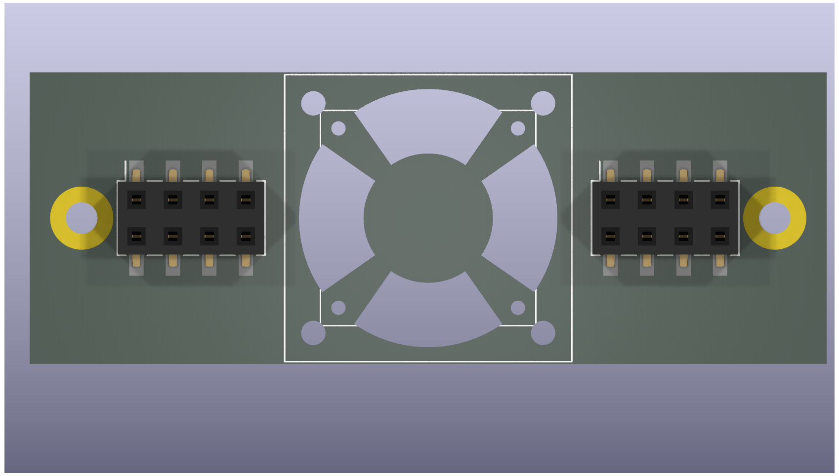
Neat. Would be handy sitting above your P2DU to blow air over the P2, although I guess you lose access to some top pins. Pity the smaller fan doesn't fit inside the 2x6 header gap. Maybe an under mount would still be possible if your board sits up more than 6.2mm from a lower PCB surface giving space for the 5mm fan to blow air around the 1.2mm P2 height. Or smaller if that tiny 3mm fan is used for example. That'd still leave height for clearing your other tallest components like the USB-C connector but you would not have the ability then to mount with solder nuts as they are blocked on that side so you'd probably need a row of though hole pins down each edge to hold it instead.
@rogloh
we faced similar stability issues with PSRAM while designing our "P2 Thing" board.
Ended up with a stable sysclock / 3 96 MB on 3 banks configuration (sysclock @ 334 Mhz).
For some reason sysclock / 2 also works reliably by using only 64 MB and disabling one bank.
If could be of any help what solved our stability issues was
In this way P2 runs also at 365 Mhz.
Top layer
Data Bus
Full copper Inner and Bottom layer for heat transportation to the exterior
Heed his words, that design runs very stable despite being in an enclosure with no cooling, not even air vents.
Interesting that the north and west sides of the copper plane are blocked by all those vias...
EDIT of note: I just noticed I have left the MXX Thing running MisoYume (at 343 MHz!) for multiple days while tending to Other EndeavoursTM and it has not crashed. Reliable engineering.
Thanks @MXX. Yes I really like your memory layout - clean consistent traces on each lane. I know Lachlan and I talked about using the USON-8 parts some time back but seemed to be hard to acquire at the time. We can look again for those. It would free up extra space on the board too such that there may be better layout options for the extra PSRAM on the board. A 6 layer board was another option but I think we needed to be at 0.8mm total thickness for the edge connector to fit nicely which limited the design with the manufacturer selected. The originally supplied PCB thickness was something even thinner like 0.7mm.
Still considering what to do but this is really useful input. Moving to USON-8 size is a good challenge to try do by hand but I would be up for it given earlier decent results with fine pitch stuff on the hotplate. Good to try to push the skillset to the next level. Along with using 0402 from 0603 etc.
Yeah that's a great result.
Looks like Mouser has some USON-8 PSRAMs in stock right now at 3.3V which is good.
However browsing the data sheet I noticed an interesting data point. It seems to say the rated performance is lower for higher voltages. This P2DU board has a higher VCC output of 3.47V IIRC which is potentially reducing performance even more. So I wonder if we drop the IO voltage down a bit whether we might get better PSRAM performance. I also question if this is the correct way around...? Usually it's the higher voltages let you overclock more, so maybe this is some thermal or peak IO slew rate issue from IO current restrictions in the device which reduces performance at higher voltages as it takes longer to fully stabilise between wider logic levels thresholds or something like that. Like how you can drive IO faster if it doesn't change the voltage as much in low voltage differential signalling systems.
I note also the APS12804 have appeared on Mouser. No stock yet, and only 1v8 available at this stage, but the APS website says these are now in MP so hopefully 3v versions are not too far away
Thanks for the useful information Mxx.
Just wired up a janky way to drop the IO voltage down to lower than 3.46. It's now set for 3.1V but can go lower than this via 2Mohm pot adjust in the feedback path of the 3.3V switching regulator.
Gonna try a few tests to see if this helps the memory performance.
At 3.1V the PSRAM seems to behave slightly differently. Previous results here https://forums.parallax.com/discussion/comment/1570101/#Comment_1570101 and here https://forums.parallax.com/discussion/comment/1570132/#Comment_1570132 tapered later than this but this version transitions to the next 14 clock delay "half-step" up at 341MHz to 350MHz, showing it still working at the higher frequencies....maybe this is actually good result despite less band overlap around 338MHz where we want to operate. The earlier results were fading out at the top end when hot too. Need to test more for some more definitive results with Wuerfel's RAM tests.
I'd say if there's only one good setting during that transition, that one might actually be better, as that'd mean it's sampling the Eye dead on center.
Good to have some proof that VIO affects PSRAM performance. Luckily it shouldn't be hard to design boards to have an extra-low VIO rail for PSRAM pins without affecting the rest of the I/O.
@rogloh
At the time I also tried PSRAM @ exactly 3.0 V to see what happens.
I didn't noticed any improvement (seems worse), don't know if it was due to the lower PSRAM voltage or the P2 IO not working well at that voltage. Cannot find any spec about P2 VIO.
About manually mounting USON-8 size should not be too difficult as they have a central pad that helps alignment.
Could you provide the piece of software used for your tests, please? The one giving the table with different delays. Thanks
I agree that so far it does seem a little worse but it hasn't been thoroughly tested yet - it didn't seem to help Wuerfel's RAM test when I tried it today, it still fails almost right away - about a minute or less. I wonder if the signal timing differences related to the lower voltage range or from reflections at different operating frequencies/delays is negatively affecting the sampling eye in this 320-340MHz operating region, but I'd need a decent scope to see that happening while the voltage is changed. Normally the half steps extend the bands and taper off one at a time, but in the case just posted above both adjacent values taper at once. I can only imagine that sort of thing is occurring if the data or clock signal is rather distorted, like overshooting/ringing etc, and not a nice clean signal transition.
Sure, here's the link to the software I use below. It's in this p2memorydrv.zip file and you want to build the file called psram_delay_test.spin2. It will run at 115200bps over the download serial port and prompts for pins and test range etc. It's setup for 32MB of PSRAM but can be tweaked to test more PSRAM fitted on other banks by just changing the chip select you input. It'd be interesting to compare with your own board to see what you get over the same range from 300-350MHz. I'd imagine it tapers between delay bands nicely vs what I'm seeing on my board.
Also I was going to ask, how are you routing the clock to your devices, is it snaking around as a single trace or do you fan it out from the P2 to each device separately from the source? Your picture seems to show rows of clock nets to each group of 3 PSRAMs per nibble but where are they connected together? Was a little hard to see that.
https://forums.parallax.com/discussion/download/137654/p2memorydrv_09b.zip
Certainly it's changing things, whether good or bad may be difficult to fully tell yet as I may have other signal issues on my board. A lower VIO rail may also reduce overall power consumption/self heating a small amount too, but PSRAMs don't burn very much power, 5.5mA was quoted at 133MHz for each device, excluding IO load current. This result may also show that large amounts of switching noise on the VIO rail of around 200-300mV or so could really affect performance by shifting the bands around a bit. So if your board is marginal to begin with the extra supply noise could potentially take you from one band to the next. That's a lot of noise though. Make me want to go scope this IO voltage supply now.
@rogloh
thanks for the test code, this is what I got on a 32 MB bank on my board
32
Enter the chip enable pin number for your PSRAM [30]: 30
Enter the clock pin number for your PSRAM [31]: 31
Enter a starting frequency to test in MHz (50-350) : [50] 300
Enter the ending frequency to test in MHz (300-350) : [350] 350
Enter 1 to use the automatic delay value only, or 0 to test over the delay range : [0] 0
Enter 1 to display the first error encountered, or 0 to not display error details : [0] 0
Testing P2 from 300000000 - 350000000 Hz

                        Successful data reads from 100 block transfers of 8192 random bytes
Frequency      Delay    3       4       5       6       7       8       9       10      11      12      13      14
300000000        (11)   0%      0%      0%      0%      0%      0%      0%      100%    100%    100%    0%      0%
301000000        (11)   0%      0%      0%      0%      0%      0%      0%      100%    100%    100%    0%      0%
302000000        (11)   0%      0%      0%      0%      0%      0%      0%      100%    100%    100%    0%      0%
303000000        (11)   0%      0%      0%      0%      0%      0%      0%      100%    100%    100%    0%      0%
304000000        (11)   0%      0%      0%      0%      0%      0%      0%      100%    100%    100%    0%      0%
305000000        (11)   0%      0%      0%      0%      0%      0%      0%      100%    100%    100%    0%      0%
306000000        (11)   0%      0%      0%      0%      0%      0%      0%      100%    100%    100%    0%      0%
307000000        (11)   0%      0%      0%      0%      0%      0%      0%      100%    100%    100%    0%      0%
308000000        (11)   0%      0%      0%      0%      0%      0%      0%      100%    100%    100%    0%      0%
309000000        (11)   0%      0%      0%      0%      0%      0%      0%      100%    100%    100%    0%      0%
310000000        (12)   0%      0%      0%      0%      0%      0%      0%      100%    100%    100%    0%      0%
311000000        (12)   0%      0%      0%      0%      0%      0%      0%      100%    100%    100%    0%      0%
312000000        (12)   0%      0%      0%      0%      0%      0%      0%      100%    100%    100%    0%      0%
313000000        (12)   0%      0%      0%      0%      0%      0%      0%      100%    100%    100%    0%      0%
314000000        (12)   0%      0%      0%      0%      0%      0%      0%      100%    100%    100%    0%      0%
315000000        (12)   0%      0%      0%      0%      0%      0%      0%      100%    100%    100%    0%      0%
316000000        (12)   0%      0%      0%      0%      0%      0%      0%      100%    100%    100%    0%      0%
317000000        (12)   0%      0%      0%      0%      0%      0%      0%      100%    100%    100%    88%     0%
318000000        (12)   0%      0%      0%      0%      0%      0%      0%      100%    100%    100%    99%     0%
319000000        (12)   0%      0%      0%      0%      0%      0%      0%      100%    100%    100%    100%    0%
320000000        (12)   0%      0%      0%      0%      0%      0%      0%      100%    100%    100%    100%    0%
321000000        (12)   0%      0%      0%      0%      0%      0%      0%      100%    100%    100%    100%    0%
322000000        (12)   0%      0%      0%      0%      0%      0%      0%      100%    100%    100%    100%    0%
323000000        (12)   0%      0%      0%      0%      0%      0%      0%      100%    100%    100%    100%    0%
324000000        (12)   0%      0%      0%      0%      0%      0%      0%      100%    100%    100%    100%    0%
325000000        (12)   0%      0%      0%      0%      0%      0%      0%      100%    100%    100%    100%    0%
326000000        (12)   0%      0%      0%      0%      0%      0%      0%      47%     100%    100%    100%    0%
327000000        (12)   0%      0%      0%      0%      0%      0%      0%      0%      100%    100%    100%    0%
328000000        (12)   0%      0%      0%      0%      0%      0%      0%      0%      100%    100%    100%    0%
329000000        (12)   0%      0%      0%      0%      0%      0%      0%      0%      100%    100%    100%    0%
330000000        (12)   0%      0%      0%      0%      0%      0%      0%      0%      100%    100%    100%    0%
331000000        (12)   0%      0%      0%      0%      0%      0%      0%      0%      100%    100%    100%    0%
332000000        (12)   0%      0%      0%      0%      0%      0%      0%      0%      100%    100%    100%    0%
333000000        (13)   0%      0%      0%      0%      0%      0%      0%      0%      100%    100%    100%    0%
334000000        (13)   0%      0%      0%      0%      0%      0%      0%      0%      100%    100%    100%    0%
335000000        (13)   0%      0%      0%      0%      0%      0%      0%      0%      100%    100%    100%    0%
336000000        (13)   0%      0%      0%      0%      0%      0%      0%      0%      100%    100%    100%    0%
337000000        (13)   0%      0%      0%      0%      0%      0%      0%      0%      100%    100%    100%    0%
338000000        (13)   0%      0%      0%      0%      0%      0%      0%      0%      100%    100%    100%    0%
339000000        (13)   0%      0%      0%      0%      0%      0%      0%      0%      100%    100%    100%    0%
340000000        (13)   0%      0%      0%      0%      0%      0%      0%      0%      100%    100%    100%    0%
341000000        (13)   0%      0%      0%      0%      0%      0%      0%      0%      100%    100%    100%    0%
342000000        (13)   0%      0%      0%      0%      0%      0%      0%      0%      100%    100%    100%    0%
343000000        (13)   0%      0%      0%      0%      0%      0%      0%      0%      100%    100%    100%    0%
344000000        (13)   0%      0%      0%      0%      0%      0%      0%      0%      100%    100%    100%    0%
345000000        (13)   0%      0%      0%      0%      0%      0%      0%      0%      100%    100%    100%    0%
346000000        (13)   0%      0%      0%      0%      0%      0%      0%      0%      100%    100%    100%    0%
347000000        (13)   0%      0%      0%      0%      0%      0%      0%      0%      100%    100%    100%    0%
348000000        (13)   0%      0%      0%      0%      0%      0%      0%      0%      100%    100%    100%    0%
349000000        (13)   0%      0%      0%      0%      0%      0%      0%      0%      100%    100%    100%    0%
350000000        (13)   0%      0%      0%      0%      0%      0%      0%      0%      100%    98%     100%    0%
350 Mhz starts looking weird...
@rogloh
From what I understood the driver runs PSRAM chips at sysclock / 2, isn't it?
@Wuerfel_21
at 334 Mhz, like in NeoYume, the delay sweet spot seems to be 12.
In NeoYume config I have to set PSRAM_DELAY = 14.
Are these two delays related somehow? Maybe PSRAM driver is different?
@rogloh
First image shows clocks and CS routing.
Second image is inner layer power supplies.
Hope this helps.
Yes, the values are not portable. Roger mixes the sync data setting in with the delay and applies some constant offset.
Yep, the tester producing max of 4 good columns per frequency confirms that. You'd get up to six good columns for sysclock/3.
The good columns for "delay" comes from, at sysclock/2:
A ) there being two possible latency alignments (lag) in raw clock intervals, and
B ) a small delay line effect is introduced via clock pin registration. So the least bit of "delay" controls enabling this registration, aka sync. Basically, this is a convenient hack for fine adjustment.
This is a general streamer <-> smartpin mashing up mechanism that the driver software has to manage. The smartpins run independently of the streamers and cogs so there is a number of steps to get the two aligned. I use the same approach for the fast 4-bit wide SD card driver code too.
Some applications have data pin registration used also but does not improve resolution of lag adjustment. It's either always on or always off.
That's such an awesome result no wonder your board is rock solid.
Yes data transfers at at half P2 (sys)clock speed, though it will transfer at a data rate of sysclock MBytes/sec for 16 bit PSRAM. Can be confusing at times if these are mixed.
Yeah as Ada mentioned my driver is different - I only had a 4 bit field to hold this delay value in the driver so I needed to add an offset to maximize the range. Plus the LSbit of this delay is actually the "half step" of the overall delay - so the full range is only 8 P2 clock cycles worth.
Thanks for the better pics. It looks like you use 1 clock column trace which feeds 4 row traces of with 3 chips(banks) per row or nibble. It's a very tidy arrangement albeit not length matched. Doesn't seem to matter as still gives a damn good result in the test. Well done.
UPDATE: Also I just measured the noise on the VIO rail - am only seeing 70mV p-p max noise or occasional worst case spikes on scope in persist mode so it's probably not that noisy. There are a lot of IO switching pins with the parallel video output but it's all pretty well bypassed on the P2DU board and the 3.3V regulator has a high 3A max output capability.
Had a rough mess about with the PCB placement and it looks more promising to fit on a single board with the smaller PSRAM chips, plus allows for the cleaner routing to the RAMs now on the right side. The uSD card reader is not the correct footprint and is just a placeholder for now; I'd use one of those slim readers with the card sitting inside above the flash chip. EDIT: alternatively I could put it back where it is meant to go facing out the side of the cartridge and move the USB-C to the top facing upwards - that would require an optional cut-out on the top edge for exposing the USB-C for debug/download and/or VGA/component out. Potentially better if you run a USB-C cable outwards towards a TV for example.
Also found that the ENIG 6 layer board is 2x the price to make over the 4 layer one I did last time (~$53 vs $26 AUD or so in 5x qty), but can actually be made in 0.8mm thickness which is good to know.