Megayyume should work out of the box after config (since it only needs one 8MB chip, anyways).
Will see if I can add 4bit support to NeoYume, but no guarantees that it's actually playable. Relatedly, slight issue: banks in @rogloh 's driver are 16MB, so I guess you can't map multiple chips as one contiguous space?
@Wuerfel_21 said:
Megayyume should work out of the box after config (since it only needs one 8MB chip, anyways).
Will see if I can add 4bit support to NeoYume, but no guarantees that it's actually playable. Relatedly, slight issue: banks in @rogloh 's driver are 16MB, so I guess you can't map multiple chips as one contiguous space?
That's correct. 16 MB is the minimum size boundary per bank in my driver. That would cause discontiguous addressing on a 4 bit setup with multiple banks done like this. You would have 8MB of memory, then an 8MB foldover portion, then the next real 8MB of memory, and its 8MB of foldover etc.
@Rayman said:
If we could get one of the small NeoYume games to work with this, would be great.
If not, I have the big one too...
Unless an 8 bit wide variant of my driver gets developed, to fill this RAM initially with data NeoYume would need two PSRAM driver COGs (or possibly one COG respawned half way through the write stage with a new data bus allocated to it). In the NeoYume arbiter COG it could be neat to try to interleave the two different groups of banks using the A23 bit of the address as the selector of which data bus to access as that could solve the 8MB issue too. A23 would choose the upper or lower 8MB of each 16MB range from the two data buses and actual address foldover could then be ignored, making the memory appear fully contiguous in NeoYume.
Not sure how fast this will run. With any luck you can get it to clock up to 169MHz. There are quite a few vias and long traces. Is there a ground plane underneath? On my own PSRAM breakout I tried to keep my board wiring very short and attempted to match clock trace lengths to each group to some extent to assist in keeping skew under control. It could work on a P2 running at around 335MHz or so IIRC, but I never soldered in the second bank of chips (was missing one device of four), so it might have slowed down more after that.
Looking at the 4 bit PSRAM driver it seems like it could be possible to hack it to support interleaving the 8MB between each sub bank of the memory, to support this 96MB layout. It would potentially take up 10 more LUT longs in the driver, and incur 5 instructions extra latency for either the read or write paths of the code. I need to read address bit A23, then patch this bit into the clock pin (odd/even 8MB selector), and also into the channel commands so the correct data bus is used by the streamer.
E.g. do this sort of thing, for read and write paths:
We only use 901 total longs in this 4 bit driver COG, so there is room for the code, only downside here is the extra 10 clocks of latency per transfer burst. Complexity is sort of hidden and each 16MB bank is split automatically into the two sub-banks seamlessly by the driver. Application wouldn't know it's not a 16MB bank, so it would appear as 6 x 16 MB banks. Only the lower clock pin of the adjacent pair would be associated with each bank. It's probably worth an attempt. NeoYume and other emulators would need to do the same thing, or if they are read only they could even use 8 bits bus reads instead of 4 bit (if the ROM data from SD is transformed and written in a way that suits this type of later access, needs some byte munging for that to work perhaps).
I was just thinking about the small 24MB board. Need a 4bit driver modified for contiguous addressing of 8MB banks.
The big board needs an 8bit driver, which makes the banks 16MB and thus doesn't have the issue to begin with.
For the little 24MB board with 3 chip selected devices, a quick hack might be to have a secondary CS pin possible as the device CS pin if A23=1. We have spare space in the pin config long for another byte. You'd then setup just 2x16MB banks in the driver and provision the CS_0 pin as the regular CS for bank0, and the CS_1 pin as the secondary CS pin for bank0. The CS_2 pin would be setup for the primary CS for bank1 and the secondary CS pin as CS_0 for bank1, so foldover would only occur in the 24-32MB space back to address 0-8MB. The code would then patch in the secondary CS_1 pin if A23=1 which is the upper half of the bank. It would only add two lines of code to the read and write paths which isn't bad.
The 96MB board is designed to support either 2x4 bit accesses (so two independent emulator COGs or my driver COGs can serve different clients simultaneously), OR alternatively as 1x8 bit for higher transfer performance (with a two pin clock pin group as the CLK). We just don't currently have a 1x8bit PSRAM driver to load memory however.
As designed the 96MB board itself is quite versatile and is a good use of the 16 available pins. An 8 bit bus driver could help it even more, we just don't have one right now for writing. Reads should be straightforward if aligned on multiples of 16 bits, writes are much harder.
Anyways, single 8MB chip support just got committed to NeoYume. Obviously only plays a handful of really small games. Crossed Swords, Fatal Fury 1, Mutation Nation and Sengoku work.
@Wuerfel_21 said:
Anyways, single 8MB chip support just got committed to NeoYume. Obviously only plays a handful of really small games. Crossed Swords, Fatal Fury 1, Mutation Nation and Sengoku work.
That's good to know from a performance point of view. It's interesting that some of these emulators are working out even with the single 4 bit chip versions. The slightly increased latency and reduced bandwidth are not such a big deal in those cases when small amounts of data is requested. Hi-res video applications on the other hand, loves all that extra bandwidth.
@Rayman said:
Is there any kind of very simple program, in Spin2 maybe, that will tell me if the boards have a pulse?
If not, guess I need to write something...
As a quick test to prove it works (but not to debug problems) you could take my 4 bit PSRAM driver stuff (attached) and the corresponding video demo and configure it to run through each chip separately for testing each one individually. It uses the VGA/AV breakout and you have to patch the pin numbers for your setup.
Eg. here in the demo file, setup the base VGA pin.
' pin setup for VGA output board
VGA_BASE_PIN = 24
and here in psram4.spin2 you setup the CLK, CE and data bus base pin numbers.
Also forgot to mention, being a new board you'll probably need to try different timing values...none of the predefined frequency profiles we have would necessarily suit your board, although you could try the automatic value, otherwise you can pass different delays into the startx method's third parameter from 1-15.
For VGA timing @252MHz, some value of delay from 9..11 is probably likely to work.
startx(freq, burst, delay, desiredcog)
This is an extended API to start the PSRAM driver using custom parameters.
freq - frequency to use for computing delay/burst sizes, or 0 to use current P2 frequency
burst - maximum memory burst size in bytes (must keep it below 8us with overheads included), 0 = automatically computed
delay - input delay value to use for the memory (0-15), 0=automatically compute based on frequency
desiredcog - a cog ID from 0-7 can be nominated for the driver cog, or will be auto allocated if it is -1
}}
@Rayman said:
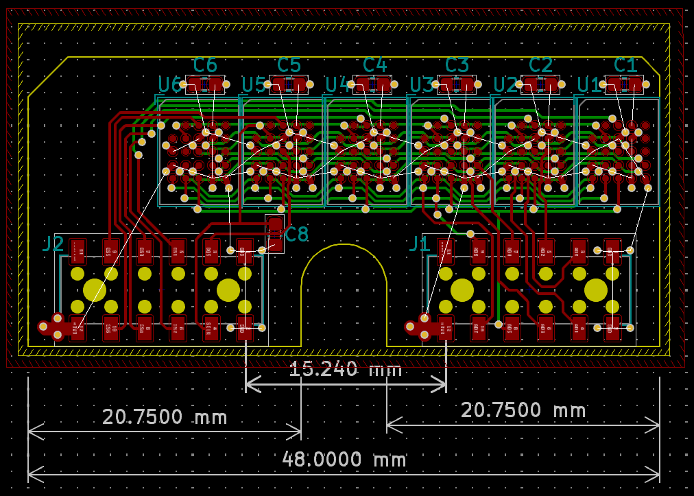
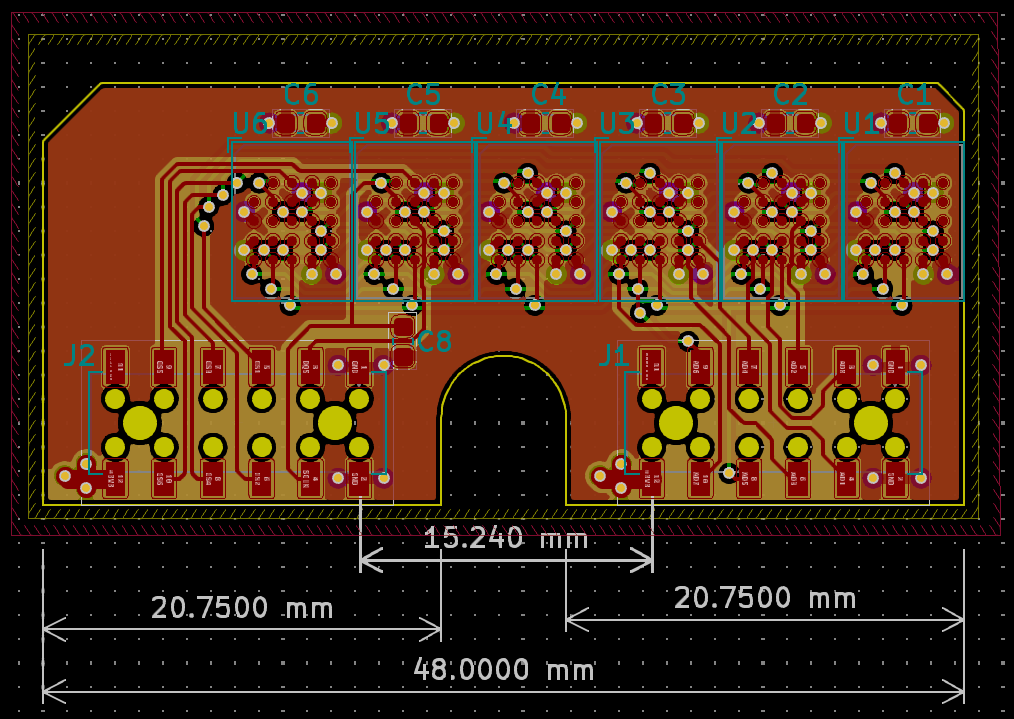
Put together one 96MB board and it passes a simple ID test.
Wish I'd labelled the banks 0..5. Have to remember to do that for next batch.
Does it work with my video test when you try individual chips in 4 bit mode? That will push it harder.
Well, I'm having some success with those tiny BGA packages after Rayman said they're a piece of cake to hand-sold. I've decide 4-layer is the only sane way to do them, and JLCPCB are offering cheap 4-layer short runs so why not.
I still need to find/change to those snazzy DIL through-board header sockets though.
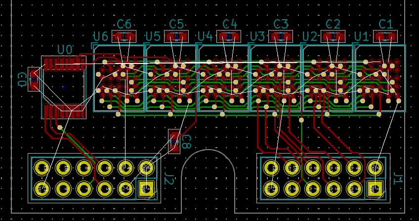
On the pours: how do you tell KiCAD’s DRC not to throw errors for the “missing” traces? I always wind-up sticking some “fake” tracks between connected pins just to satisfy the DRC (These tracks then get covered by the pour).
I don't run the DRC. It complains too much about the outlines overlapping. I'm happy with interactive copper clearances for keeping me on the right track. ... I see the DRC is reporting one error where C8 overlaps the connector. I know that has enough room in reality.
Interestingly, the unconnected VSS/VDD nets aren't reported in the DRC report. The two fill zones are spec'd for VSS and VDD so sensibly they are accounted for, I presume. But there is a bunch of data tracks reported as unconnected at various vias ... EDIT: Nothing wrong with them! All tracks are connected to those vias.
EDIT2: Ah, lots of VSS/VDD are reported when the fillszones are not filled in, ie: when CTRL-B'd
EDIT3: I did change the board setup part way through, from a 2-layer to a 4-layer. I got my four layers, and no odd-ball behaviour resulted. Shrug, dunno why it's got warnings at some of the vias.
@rogloh Seems your video demo works, thanks! This is testing one of three chips on the 24 MB board. Thought I would have to use CE on the other two chips to make sure they are not enabled, but don't seem to need to.
@Rayman said:
@rogloh Seems your video demo works, thanks! This is testing one of three chips on the 24 MB board. Thought I would have to use CE on the other two chips to make sure they are not enabled, but don't seem to need to.
Great. Yeah pull ups are useful on CE pins when there is nothing driving them. At driver init time I do drive all banks CS pins high, so once that occurs things should be safe.


Comments
Megayyume should work out of the box after config (since it only needs one 8MB chip, anyways).
Will see if I can add 4bit support to NeoYume, but no guarantees that it's actually playable. Relatedly, slight issue: banks in @rogloh 's driver are 16MB, so I guess you can't map multiple chips as one contiguous space?
If we could get one of the small NeoYume games to work with this, would be great.
If not, I have the big one too...
That's correct. 16 MB is the minimum size boundary per bank in my driver. That would cause discontiguous addressing on a 4 bit setup with multiple banks done like this. You would have 8MB of memory, then an 8MB foldover portion, then the next real 8MB of memory, and its 8MB of foldover etc.
Unless an 8 bit wide variant of my driver gets developed, to fill this RAM initially with data NeoYume would need two PSRAM driver COGs (or possibly one COG respawned half way through the write stage with a new data bus allocated to it). In the NeoYume arbiter COG it could be neat to try to interleave the two different groups of banks using the A23 bit of the address as the selector of which data bus to access as that could solve the 8MB issue too. A23 would choose the upper or lower 8MB of each 16MB range from the two data buses and actual address foldover could then be ignored, making the memory appear fully contiguous in NeoYume.
Not sure how fast this will run. With any luck you can get it to clock up to 169MHz. There are quite a few vias and long traces. Is there a ground plane underneath? On my own PSRAM breakout I tried to keep my board wiring very short and attempted to match clock trace lengths to each group to some extent to assist in keeping skew under control. It could work on a P2 running at around 335MHz or so IIRC, but I never soldered in the second bank of chips (was missing one device of four), so it might have slowed down more after that.
Looking at the 4 bit PSRAM driver it seems like it could be possible to hack it to support interleaving the 8MB between each sub bank of the memory, to support this 96MB layout. It would potentially take up 10 more LUT longs in the driver, and incur 5 instructions extra latency for either the read or write paths of the code. I need to read address bit A23, then patch this bit into the clock pin (odd/even 8MB selector), and also into the channel commands so the correct data bus is used by the streamer.
E.g. do this sort of thing, for read and write paths:
                            testb cmdaddr, #23 wc
                            bitc clkpin, #0
                            bitc ximm8, #19
                            bitc xrecvdata, #19
                            bitc xsendimm, #19
We only use 901 total longs in this 4 bit driver COG, so there is room for the code, only downside here is the extra 10 clocks of latency per transfer burst. Complexity is sort of hidden and each 16MB bank is split automatically into the two sub-banks seamlessly by the driver. Application wouldn't know it's not a 16MB bank, so it would appear as 6 x 16 MB banks. Only the lower clock pin of the adjacent pair would be associated with each bank. It's probably worth an attempt. NeoYume and other emulators would need to do the same thing, or if they are read only they could even use 8 bits bus reads instead of 4 bit (if the ROM data from SD is transformed and written in a way that suits this type of later access, needs some byte munging for that to work perhaps).
I was just thinking about the small 24MB board. Need a 4bit driver modified for contiguous addressing of 8MB banks.
The big board needs an 8bit driver, which makes the banks 16MB and thus doesn't have the issue to begin with.
For the little 24MB board with 3 chip selected devices, a quick hack might be to have a secondary CS pin possible as the device CS pin if A23=1. We have spare space in the pin config long for another byte. You'd then setup just 2x16MB banks in the driver and provision the CS_0 pin as the regular CS for bank0, and the CS_1 pin as the secondary CS pin for bank0. The CS_2 pin would be setup for the primary CS for bank1 and the secondary CS pin as CS_0 for bank1, so foldover would only occur in the 24-32MB space back to address 0-8MB. The code would then patch in the secondary CS_1 pin if A23=1 which is the upper half of the bank. It would only add two lines of code to the read and write paths which isn't bad.
E.g this:
testb cmdaddr, #23 wc if_c getbyte cspin, pinconfig, #2 ' override CS pin with secondary CS pinThe 96MB board is designed to support either 2x4 bit accesses (so two independent emulator COGs or my driver COGs can serve different clients simultaneously), OR alternatively as 1x8 bit for higher transfer performance (with a two pin clock pin group as the CLK). We just don't currently have a 1x8bit PSRAM driver to load memory however.
As designed the 96MB board itself is quite versatile and is a good use of the 16 available pins. An 8 bit bus driver could help it even more, we just don't have one right now for writing. Reads should be straightforward if aligned on multiples of 16 bits, writes are much harder.
Yeah, as I said, you gotta make an 8bit driver. Can use one 48MB half in the meantime though.
(Anyways, currently trying to make single 4bit PSRAM NeoYume happen, multibank can come after that, but I can't test it without hardware)
I'll send you all a PM about sample boards.
Is there any kind of very simple program, in Spin2 maybe, that will tell me if the boards have a pulse?
If not, guess I need to write something...
Anyways, single 8MB chip support just got committed to NeoYume. Obviously only plays a handful of really small games. Crossed Swords, Fatal Fury 1, Mutation Nation and Sengoku work.
That's good to know from a performance point of view. It's interesting that some of these emulators are working out even with the single 4 bit chip versions. The slightly increased latency and reduced bandwidth are not such a big deal in those cases when small amounts of data is requested. Hi-res video applications on the other hand, loves all that extra bandwidth.
As a quick test to prove it works (but not to debug problems) you could take my 4 bit PSRAM driver stuff (attached) and the corresponding video demo and configure it to run through each chip separately for testing each one individually. It uses the VGA/AV breakout and you have to patch the pin numbers for your setup.
Eg. here in the demo file, setup the base VGA pin.
    ' pin setup for VGA output board

    VGA_BASE_PIN = 24
and here in psram4.spin2 you setup the CLK, CE and data bus base pin numbers.
    ' P2 EDGE with PSRAM pin mappings (P2-EC32MB)
    DATABUS  = 40
    CLK_PIN  = 56
    CE_PIN   = 57
Also you could change to 1024x768 video mode (or 800x600) from 640x480 if you want to test with other P2 frequencies.
Eg. change
    XSIZE = 640
    YSIZE = 480
    BPP   = 8 ' colour bit depth

    RESOLUTION = vid.RES_640x480    ' this should match the above
to
    XSIZE = 1024
    YSIZE = 768
    BPP   = 8 ' colour bit depth

    RESOLUTION = vid.RES_1024x768    ' this should match the above
In this demo, I think only 8bpp colour mode was specifically supported.
Also forgot to mention, being a new board you'll probably need to try different timing values...none of the predefined frequency profiles we have would necessarily suit your board, although you could try the automatic value, otherwise you can pass different delays into the startx method's third parameter from 1-15.
For VGA timing @252MHz, some value of delay from 9..11 is probably likely to work.
startx(freq, burst, delay, desiredcog) This is an extended API to start the PSRAM driver using custom parameters. freq - frequency to use for computing delay/burst sizes, or 0 to use current P2 frequency burst - maximum memory burst size in bytes (must keep it below 8us with overheads included), 0 = automatically computed delay - input delay value to use for the memory (0-15), 0=automatically compute based on frequency desiredcog - a cog ID from 0-7 can be nominated for the driver cog, or will be auto allocated if it is -1 }}I just wrote this simple .spin2 test program to check EID and KGD values.
Not a real good test, but should catch major blunders:
Put together one 96MB board and it passes a simple ID test.
Wish I'd labelled the banks 0..5. Have to remember to do that for next batch.
768 MEGABIT POWER!
Does it work with my video test when you try individual chips in 4 bit mode? That will push it harder.
You posted that in this thread right ?
I’ll give it a try..
Yeah around 6 posts ago #74/75.
Well, I'm having some success with those tiny BGA packages after Rayman said they're a piece of cake to hand-sold. I've decide 4-layer is the only sane way to do them, and JLCPCB are offering cheap 4-layer short runs so why not.
I still need to find/change to those snazzy DIL through-board header sockets though.
To help with the "find" part: Harwin Inc : M20-7810645
Yay, it exists in Kicad. Thank you!
EDIT: Oh, and I had the old ones upside down. That's saved me a definite revision.
Done. Kicad files attached.
On the pours: how do you tell KiCAD’s DRC not to throw errors for the “missing” traces? I always wind-up sticking some “fake” tracks between connected pins just to satisfy the DRC (These tracks then get covered by the pour).
I don't run the DRC. It complains too much about the outlines overlapping. I'm happy with interactive copper clearances for keeping me on the right track. ... I see the DRC is reporting one error where C8 overlaps the connector. I know that has enough room in reality.
Interestingly, the unconnected VSS/VDD nets aren't reported in the DRC report. The two fill zones are spec'd for VSS and VDD so sensibly they are accounted for, I presume. But there is a bunch of data tracks reported as unconnected at various vias ... EDIT: Nothing wrong with them! All tracks are connected to those vias.
EDIT2: Ah, lots of VSS/VDD are reported when the fillszones are not filled in, ie: when CTRL-B'd
EDIT3: I did change the board setup part way through, from a 2-layer to a 4-layer. I got my four layers, and no odd-ball behaviour resulted. Shrug, dunno why it's got warnings at some of the vias.
Did I say easy to hand solder? I always use a stencil. Place by hand though. Rework with hot air gun usually works when needed.
Hehe, yeah, may not be using a soldering iron but it's not using a pick'n'place machine so it's still hand soldering to me.
@rogloh Seems your video demo works, thanks! This is testing one of three chips on the 24 MB board. Thought I would have to use CE on the other two chips to make sure they are not enabled, but don't seem to need to.
Great. Yeah pull ups are useful on CE pins when there is nothing driving them. At driver init time I do drive all banks CS pins high, so once that occurs things should be safe.