@jdolecki said:
When I connect a MOSFET to an output pin is there any other components to protect the output pin or the Mosfet? Thank john
YMMV, but I'm driving 24 volts/10 amps with nothing more than a raw P2 pin connected to the gate of an IRLF44. Works nice. Nothing else needed. (Note: this is a low-side driver)
@rbehm said:
I would add a pull-down resistor to avoid an undefined state during power up when the pin is still defined as an input.
Absolutely. A floating gate is a capricious creature and a recipe for problems.
I guess I should have been more clear in my response when I said "nothing else needed". I meant nothing else was needed between the pin and the mosfet gate for protection of the P2. Of course the usual things like pullups, flyback diodes, caps to slow edge rise/fall for EMI prevention, etc, do need careful consideration.
When you connect the gate of a MOSFET to a Propeller pin, that MOSFET better have a very low VGS drive requirement. And don't just look at the VGS threshold voltage in the data sheet: that's not the whole story. There will also be graphs that show source-drain current versus gate voltage. Your own drive current requirements at VGS=3.3V had better be well below that curve if you don't want the transistor to get hot.
This is the IRLF44 transfer curve. Not to hijack the thread, but I’m looking for something a bit beefier at 3.0 volts gate to source, if anyone has any suggestions.
I’m a victim of big fingers/small keyboard/decaffinated brain.
I can totally relate. I type most of my forum comments on a MacBook. I hate that freaking keyboard! It's like typing on a pillow: no tactile feedback at all, resulting in scads of missing characters. By contrast, the keyboard on my shop computer is an original IBM model M with "clicky keys" like those of their Selectric typewriters. It's very heavy -- built like a tank. I love it!
Phil: I recently borrowed an “old school”/“retro” keyboard from my son. It uses discrete Cherry switches that are replaceable. About $130 (!!!) but I nearly didnt give it back. It feels WONDERFUL and has all the right tactile feedback. Check these out if you love the “old” feel!
@rbehm said:
I would add a pull-down resistor to avoid an undefined state during power up when the pin is still defined as an input.
Absolutely. A floating gate is a capricious creature and a recipe for problems.
I guess I should have been more clear in my response when I said "nothing else needed". I meant nothing else was needed between the pin and the mosfet gate for protection of the P2. Of course the usual things like pullups, flyback diodes, caps to slow edge rise/fall for EMI prevention, etc, do need careful consideration.
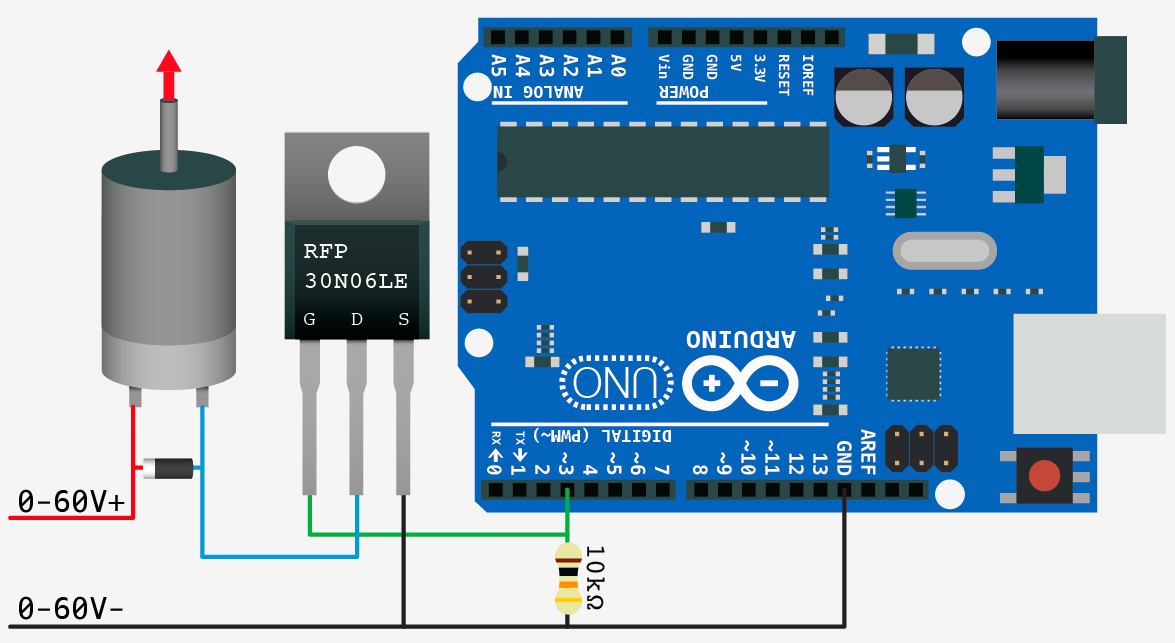
That’s what I need to know is there a pin to mosfet schematic is there a sample schematic I could see?
@jdolecki said:
When I connect a MOSFET to an output pin is there any other components to protect the output pin or the Mosfet? Thank john
As above, the mosfet GATE does not strictly need protecting, but you may want to protect the DRAIN pin, with a flyback diode or a clamp Zener.
Some designs use a series gate resistor which slows things down, to trade off better EMC with slightly higher switching edge losses.
You do need to check the gate drive specs, especially for 3v3 drive. See below.
@JRoark said:
This is the IRLF44 transfer curve. Not to hijack the thread, but I’m looking for something a bit beefier at 3.0 volts gate to source, if anyone has any suggestions.
Ideally you want a part actually specified for 3.3V gate drive, but at also 50V, those are not so common, at the tens of amps region.
If you do sort by parts spec'd at 2.5V drive, the highest VDS offered by OnSemi is 30V
ie at 2.5V gate drive, it seems 30V is your top end for VDS.
If you need higher VDS, than 30V, then a gate drive buffer is needed, allowing a 4v or 4.5V spec'd MOSFET.
Data says : FDMC86012: N-Channel Power Trench® MOSFET 30V, 88A, 2.7mΩ
This device has been designed specifically to improve the efficiency of DC-DC converters. Using new techniques in MOSFET construction, the various components of gate charge and capacitance have been optimized to reduce switching losses. Low gate resistance and very low Miller charge enable excellent performance with both adaptive and fixed dead time gate drive circuits. Very low rDS(on) has been maintained to provide a sub logic-level device.
Max rDS(on) = 2.7 mΩ at VGS = 4.5 V, ID = 23 A
Max rDS(on) = 4.7 mΩ at VGS = 2.5 V, ID = 17.5 A
and FDMC8651: N-Channel Power Trench® MOSFET 30V, 20A, 6.1mΩ
This device has been designed specifically to improve the efficiency of DC/DC converters. Using new techniques in MOSFET construction, the various components of gate charge and capacitance have been optimized to reduce switching losses. Low gate resistance and very low Miller charge enable excellent performance with both adaptive and fixed dead time gate drive circuits. Very low rDS(on) has been maintained to provide a sub logic-level device.
Max rDS(on) = 6.1 mΩ at VGS = 4.5 V, ID = 15 A
Max rDS(on) = 9.3 mΩ at VGS = 2.5 V, ID = 12 A
@jdolecki said:
Last question if I want the Mosfet output to be positive to the load and the other side of the load grounded what type of Mosfet should I use.
A lot of the example I see are Mosfet output to negative.
@jdolecki said:
Last question if I want the Mosfet output to be positive to the load and the other side of the load grounded what type of Mosfet should I use.
A lot of the example I see are Mosfet output to negative.

 jdolecki
Posts: 726
jdolecki
Posts: 726

Comments
YMMV, but I'm driving 24 volts/10 amps with nothing more than a raw P2 pin connected to the gate of an IRLF44. Works nice. Nothing else needed. (Note: this is a low-side driver)
I would add a pull-down resistor to avoid an undefined state during power up when the pin is still defined as an input.
Absolutely. A floating gate is a capricious creature and a recipe for problems.
I guess I should have been more clear in my response when I said "nothing else needed". I meant nothing else was needed between the pin and the mosfet gate for protection of the P2. Of course the usual things like pullups, flyback diodes, caps to slow edge rise/fall for EMI prevention, etc, do need careful consideration.
When you connect the gate of a MOSFET to a Propeller pin, that MOSFET better have a very low VGS drive requirement. And don't just look at the VGS threshold voltage in the data sheet: that's not the whole story. There will also be graphs that show source-drain current versus gate voltage. Your own drive current requirements at VGS=3.3V had better be well below that curve if you don't want the transistor to get hot.
-Phil
This is the IRLF44 transfer curve. Not to hijack the thread, but I’m looking for something a bit beefier at 3.0 volts gate to source, if anyone has any suggestions.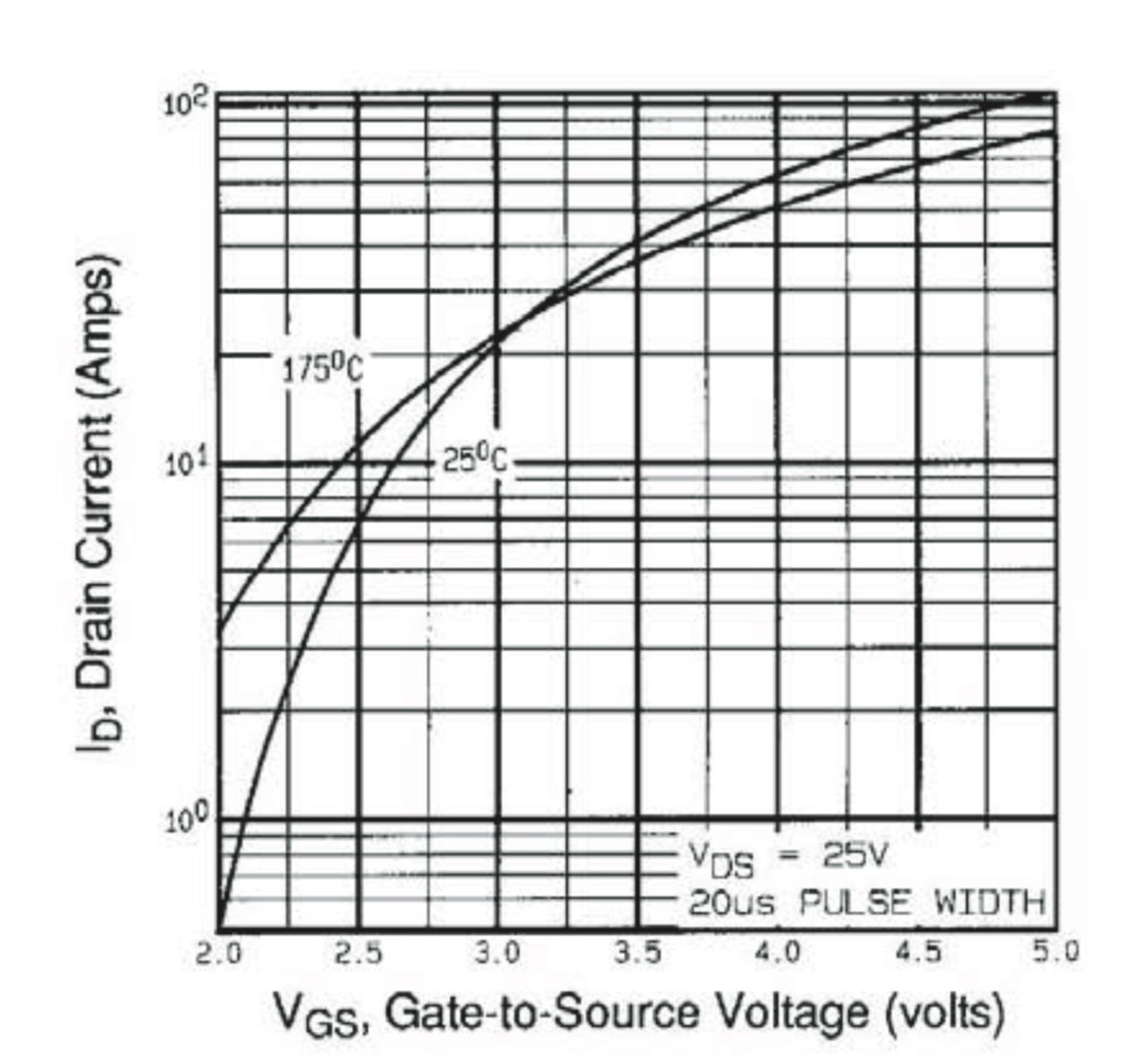
I think you mean IRLZ44, right?
-Phil
Sorry. You are correct. I’m a victim of big fingers/small keyboard/decaffinated brain. Lol
I can totally relate. I type most of my forum comments on a MacBook. I hate that freaking keyboard! It's like typing on a pillow: no tactile feedback at all, resulting in scads of missing characters. By contrast, the keyboard on my shop computer is an original IBM model M with "clicky keys" like those of their Selectric typewriters. It's very heavy -- built like a tank. I love it!
-Phil
Phil: I recently borrowed an “old school”/“retro” keyboard from my son. It uses discrete Cherry switches that are replaceable. About $130 (!!!) but I nearly didnt give it back. It feels WONDERFUL and has all the right tactile feedback. Check these out if you love the “old” feel!
it is even worse,
the company having the nicest Keyboards currently (IMHO) is called CORSAIR sounds almost like CORVAIR...
Mike
That’s what I need to know is there a pin to mosfet schematic is there a sample schematic I could see?
As above, the mosfet GATE does not strictly need protecting, but you may want to protect the DRAIN pin, with a flyback diode or a clamp Zener.
Some designs use a series gate resistor which slows things down, to trade off better EMC with slightly higher switching edge losses.
You do need to check the gate drive specs, especially for 3v3 drive. See below.
Ideally you want a part actually specified for 3.3V gate drive, but at also 50V, those are not so common, at the tens of amps region.
If you do sort by parts spec'd at 2.5V drive, the highest VDS offered by OnSemi is 30V
ie at 2.5V gate drive, it seems 30V is your top end for VDS.
If you need higher VDS, than 30V, then a gate drive buffer is needed, allowing a 4v or 4.5V spec'd MOSFET.
Data says :
FDMC86012: N-Channel Power Trench® MOSFET 30V, 88A, 2.7mΩ
This device has been designed specifically to improve the efficiency of DC-DC converters. Using new techniques in MOSFET construction, the various components of gate charge and capacitance have been optimized to reduce switching losses. Low gate resistance and very low Miller charge enable excellent performance with both adaptive and fixed dead time gate drive circuits. Very low rDS(on) has been maintained to provide a sub logic-level device.
Max rDS(on) = 2.7 mΩ at VGS = 4.5 V, ID = 23 A
Max rDS(on) = 4.7 mΩ at VGS = 2.5 V, ID = 17.5 A
and
FDMC8651: N-Channel Power Trench® MOSFET 30V, 20A, 6.1mΩ
This device has been designed specifically to improve the efficiency of DC/DC converters. Using new techniques in MOSFET construction, the various components of gate charge and capacitance have been optimized to reduce switching losses. Low gate resistance and very low Miller charge enable excellent performance with both adaptive and fixed dead time gate drive circuits. Very low rDS(on) has been maintained to provide a sub logic-level device.
Max rDS(on) = 6.1 mΩ at VGS = 4.5 V, ID = 15 A
Max rDS(on) = 9.3 mΩ at VGS = 2.5 V, ID = 12 A
http://gammon.com.au/motors
Last question if I want the Mosfet output to be positive to the load and the other side of the load grounded what type of Mosfet should I use.
A lot of the example I see are Mosfet output to negative.
Hope I said that correctly.
This is my first time using Mosfet.
There are two routes you could take:
-Phil
The link I posted?
that’s it thanks
That's a plus, Tough Guy!
It's good enough for the final episode of Stranger Things...
It took me more than it should to get (or not get) the idea of the picture.... ahh my Friday brain I think it's done or/and my eyes
