

Specifications missing in the data sheet
 ManAtWork
Posts: 2,369
ManAtWork
Posts: 2,369
I recently tried to find out what's the "official" maximum clock frequency the P2 can run. I found out that this is not clearly specified in the current data sheet. In fact, almost nothing is clearly specified! In the "AC Characteristics" there are only two parameters listed. And to me it's not clear if the maximum frequency of 320MHz is really the frequency the processor is guaranteed to operate reliably over the full temperature and supply voltage range. I think it's not and the 320MHz max is only the limit for the PLL.
In my opinion, if the P2 is to be taken seriously for any commercial product then there have to be a lot more specifications in the data sheet a disigner can count on. I know, most of us here in the forum are hobbyists or "hackers" who don't care much about paperwork and simply try out how far they can go. But if you work for a company you need to decide if this chip fits your requirements or not. You can't just invest man months of development and later find out that your product only works due to "good luck".
I know, not all parameters are tested or can be guaranteed. But even if a limit is only specified as "typical" value it helps estimating what is possible and what is not.
So here is my wish list what should be included in the data sheet:
- max. clock frequency for reliable operation over full temperature and supply voltage range
- typical overclocking capability in a narrower but well defined range
- ADC performance: max. gain and offfset error (calibrated), typical SNR for at least one set of conditions (sample rate, resolution, filter mode, gain mode)
- DAC performance: max gain and offset error, -3dB cutoff frequency
- tolerances for low-level pin drive modes (1.5k to 150k pullup/pulldown, 10uA to 1mA current)
- levels and tolerances for schmitt trigger and comperator input modes
Anything else?
Comments
The max clock is quite dependant on power consumption. Software can vary the Prop2's power needs by quite a wide margin. It's not very easy to put an exact number on max frequency. The 320 MHz is okay for low level power usage but will need qualification at a later date. On top of ambient and package temperatures, loading, thermal resistance and cooling will be factors in the qualifications.
It'll start from a linear graph for junction temperature vs PLL limit. So, first factor is already dynamic result.
Probably the original design 180 MHz target is the guaranteed number. OnSemi tools said 175 MHz was max reliable clock for the design criteria. I'm guessing 105 °C ambient was one design criteria given to them.
ADC tops out at about 12 or 13 bits under best conditions.
DAC is similar apparently. The monotonic linearity is significantly better than its native 8-bit resolution.
Both are dependant on quality VIO/GIO supply rails.
You're right of course. Still more work needed for the datasheet ... Looking at the one-page "spec sheet" I see it says 16-bit, 3 ns DACs. I think that should say 8-bit. Maybe with (dithered 16-bit) in brackets.
Another marketing blurb should be "highly symmetrical".
And on that one-page spec sheet, can replace all occurrences of "cog" with "core".
The Xoroshiro128 hardware is free running.
These aren't right at all, or at least need rewritten:
Counter modes are in the 64 smartpins, not the 8 cogs. Quadrature Decoder is one of them. The CT system counter is separate and should be listed separately.
Six 32-bit clock modes? I have no idea what that is. Maybe the sysclock source select. But there is only four of those. There is already earlier details: "Internal ~20 MHz and ~20 kHz RC oscillators. External clock input with internal loading caps. Fractional PLL, 3 stage. Frequency 180 MHz typical, 320 MHz extended."
Digital input filter is just the deglitcher circuit. That's overly optimistic to call it a filter.
Math is in the CORDIC solver. Which is already listed as eight-function earlier.
Thanks Evanh for answering some of my questions. That helps me, but I'm more concerned about the commercial success of Parallax marketing the P2. IMHO it doesn't help answering questions here in the forum. The answers have to be in the data sheet that everyone can download when he/she sees the chip on Mouser, RS or DigiKey. That is something only Parallax can do.
Totally agreed. It's impossible to guarantee a certain value for all possible cases. But other data sheets normally list test conditions. For example, a MOSFET is specified for 10A continous current at 25°C case temperature or for 6A at 100°C heatsink temperature. Not all specifications in all data sheets make sense. But if the exact test conditions are documented you have at least something you can compare to.
I'm partly expanding on what you've started - Highlighting things for Parallax to improve. Jeff may not read the forums but many others do. Particularly Chip.
The issue of insufficient documentation has been brought up numerous times already.
I will be dead honest and it will be maybe too harsh but let me say this: while the P2 is a wonderful chip it will not succeed on the commercial marketplace without proper documentation. Period.
And you're not the first to say that. It's hardly rocket science but also of no help.
True. I have said that for the last time and will never bring that subject back.
Unfortunately only Parallax themselves can fix that once and for good if and when they decide to do so. But that has also been said already.
I am not criticizing them at all. These are their business decisions and priorities I respect and all of us here (me for sure) would really like to see the P2 shine on the market and stay there for a long time as the P1 did. It would just be much easier and quicker if the issue was resolved.
Everything takes time.
I noticed the same thing. The clock rate is very poorly defined.The fact is, this will remain a hobbiest product until there are decent specifications available. There is no way that anyone is going to invest significant money and resources into a product using it as it sits. Think about it. I buy some of these and build some hardware. First off, I have to spend months to see if it will even work. Maybe I can count on 180Mhz. Ok, Then that is the maximum clock rate. The "Up to 320" is meaningless marketing doublespeak. If I buy one, put it on a board and manage the power dissipation to keep it within 2.5 watts can I be guaranteed that it will clock at 320? If so, say that. If not, dont even print that. Does intel sell you a cpu and say that it will "Probably clock at 3.8GHz but it might go as high as 5" Probably and might dont work if you want me to order 20,000 of them.
What Im worried about by those loosey goosey handwaving specs is that I might get one, and spend a whole lot of time designing something and then find out that half of them fail miserably in production or worse still, 20% fail marginally in the customers hands. And then parallax is going to say "hey, we never SAID it would do that" Unless they tell me in writing that it meets a particular specification, I cant count on any particular device meeting it.
Typically what is done is that a large number of devices in production are tested against various specifications. In the early days a very large number. As the product ramps up and its learned that they consistently meet the specifications the sample sizes can be reduced to more manageable levels.
Well, that comes as news to me (10k into physical R&D costs in one commercial project, and I’m already shipping another), not to mention a few others.
But please, do continue…")
I share your frustration with the docs. This is currently a serious weakness, but “winter is coming” for those who cite this as their reason not to dev with the P2.
Btw: what Parallax spent on the entire P2 effort, Intel spent on their design on the shipping box. Its really an “apples and oranges” comparison IMHO.
Edited to add: with 7 cores screaming along at 320 mhz, and ambient temperatures under 140F, I have not had a single failure. For those gadgets who must live in a refinery setting (ie, hotter than Satans armpits), I pulled the clock back to 250 mhz and found the other components typically fail before the P2 misses a beat. YMMV
Certainly, 'proper' data sheets have minimum and typical values.
The P2 design MHz is 175-180MHz as mentioned above, but that is a PVT limit, and IIRC at 125'C TJ. Most would consider that excessively conservative.
250MHz seems to be routinely used typical, tho current consumption varies with code & core use, and that sets how much the die & PCB elevates above TA.
ie not all 250MHz are equal, and some may need more aggressive thermal spread attention.
Parallax should be able to publish typical curves over a number of units, and is hopefully collecting histogram plots from their ATE test equipment, for every P2 chip that is tested ?")
I'm not sure if they are onto a second wafer run yet, it would be interesting to see some run-run comparisons a year or two apart
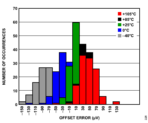
Here are some good examples of typical data presentation :
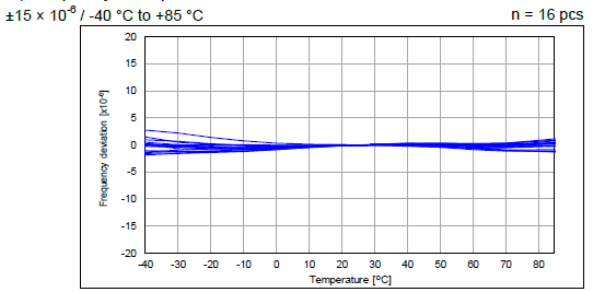
This from Epson SG-8101CG series for 16 samples of a ±15ppm MAX part (that includes 'everything' : initial frequency tolerance, temperature variation, supply voltage variation, reflow drift, load drift and aging (+25℃, 1 year)
and this histogram example from TI for ADC performance over > 100 parts, shows tempco too.
You actually will find loose specs in those overclocking /gaming markets, and they charge premium money in that area too")
Related to that, I was watching a XBOX power design video the other day, and that claimed Microsoft can and do set every one of the many core rails precisely and separately for every unit made.
I'm not sure how much of that is to track the process or measured ability, or how much is because they do not have production silicon until very late in the design cycle, or how much is to allow them to deliberately cripple/overclock models for marketing reasons")
In a room temperature I tested - many hours - a 1024x576 HDMI driver @ 357 MHz, without any stability problem. I managed to run a simple code - a sine wave generator - up to 410 MHz (requested), to discover the PLL gives up somewhere between 390 and 400 MHz.
All more complex examples which I tried to run are unstable over 380 MHz.
I am curious what a liquid nitrogen cooling can do with the chip, but of course I have no equipment to test it")
The 180 MHz rating is way too conservative, especially considering the TMDS encoder would be really pointless if it couldn't run at 250 MHz and up.
The TMDS encoder, being a very late (Rev B ) addition, certainly wasn't a planned feature.
410 MHz from the PLL will be achievable somewhere around zero centigrade I'd guess. Chiller packs surrounding the Eval board were good enough for short bursts during testing. But to run sustained would need more robust heat transfer than ambient convection provides.
Personally, I get more of a warm and fuzzy from case studies like those above.
Would love to hear more.

One area of P2 that needs better specs, is the clock-quantize influence on delays to/from the pins.
Many of the examples cannot work at any-sysclk-speed, without code adjustments, and that means an eye-diagram must exist for CLK-Temperature tolerance.
What examples? Are you meaning ones like HyperRAM and SPI at high data rates?
Yes, anything that needs to compensate for the transit times with clock adders.
Found it, here it is in nice graphical form :
https://forums.parallax.com/discussion/comment/1498092/#Comment_1498092
These plots do not include temperature ranges, so I'm saying an ideal data sheet would include these plots, with temperature spreading included to give eye patterns.
In some cases, it could even need Vdd spreading too, if you have fixed sysclks and you want to centre the eye pattern at that for best tolerance.
In another thread I mentioned a XBOX power design video, where Microsoft claimed they can, and do, fractionally tune Vcc for every single console. Amazing really.") ) so they use this to centre their eye patterns ?
) so they use this to centre their eye patterns ?
Maybe XBOX has similar transit time / high clock issues (only moved up the freq axis
I just got 435 MHz at -8.0 C. Not doing any work though. Just setting the clock frequency and waiting for a character from comport.
PS: BTW, that's the self-limiting frequency of the PLL. So it isn't entirely stable, wobbling with temperature and all. I set 440 MHz and just watched the temperature gauge and P56 frequency slowly move together.
Try a sine wave generator Output it to DACs and you can hear the main clk frequency change.
My measured frequency is accurate. Pin P56 is programmed to sysclock/1000 square wave, so I can watch it step change as I set different rates in software - Agrees to about five decimal digits.
Or in the case of PLL limited I can watch the frequency drift as the temperature changes. This has some small visible jitter on the scope.
For temperature measurement, I have a thermocouple soldered to the middle-bottom of Eval Board, right under the Prop2's exposed pad.
For temperature control I use freezer packs and a bag to keep the chilled air contained.
Yes, but hearing what is going on is simply fun.")
oh, I see. ha, but don't hear")
THIS. I worked for some years with a gizmo that required constant alignment. One day, on a whim, someone stuck a VCO (voltage-controlled oscillator, in audio frequency ranges) and a cheap little speaker on the signal. Better alignment, higher pitch...
It made aligning the bloody thing fun! wooWHEEEwoo oops, wooWHEE that's got it...
So much better than having to constantly check the voltmeter.
S.
Hehe, just been reading a "key features brief" from Micron about DDR5 DIMMs. Has a couple of sections on run-time tuning of the timings.