Also, @evanh, I've modified the routine below that determines the PLL parameters to try to use your suggestion... am testing further but it still seems to work.
MAXCLK_HZ is now set to 350000000
MAXVCO_HZ is now set to 250000000 (if I set only to 200MHz, it would fail to allow certain integer MHz frequencies).
PRI computeClockMode(desiredHz) : mode | vco, finput, fr, p, div, m, error, bestError
    bestError := -1
    repeat p from 0 to 30 step 2
        ' compute the ideal VCO frequency fr at this value of P
        if p <> 0
            if desiredHz > MAXVCO_HZ/p ' test it like this to not overflow
                quit
            fr := desiredHz * p
        else
            fr := desiredHz
            if fr > MAXCLK_HZ
                quit
        ' scan through D values, and find best M, retain best case
        repeat div from 1 to 64
            'compute the PLL input frequency from the crystal through the divider
            finput := xtal/div
            if finput < MINPLLIN_HZ ' input getting too low, and only gets lower so quit now
                quit

            ' determine M value needed for this ideal VCO frequency and input frequency
            m := fr / finput
    '       send("trying p=",f.unsdec(p), " d=", f.unsdec(div), " m=", f.unsdec(m),13,10)

            ' check for the out of divider range case
            if m +> 1024
                quit

            ' zero is special and gets a second chance
            if m == 0
                m++

            ' compute the actual VCO frequency at this particular M, D setting
            vco := finput * m
            if vco +< MINVCO_HZ
                next
            if vco +> MAXCLK_HZ
                next

            ' compute the error and check next higher M value if possible, it may be closer
            error := abs(fr - vco)
            if m < 1024 and (vco + finput) +< MAXCLK_HZ
                if error > abs(fr - (vco + finput))
                    error := abs(fr - (vco + finput))
                    m++

            ' retain best allowed frequency error and divider bits found so far
            if error +< bestError and error +< TOLERANCE_HZ+1
                bestError := error
                mode := ((div-1) << 18) + ((m-1) << 8) + (((p/2 - 1) & $f) << 4)
                mode |= (1<<24) ' enable PLL

            ' quit whenever perfect match found
            if bestError == 0
                quit

        if bestError == 0
            quit

    ' final clock mode format is this #%0000_000E_DDDD_DDMM_MMMM_MMMM_PPPP_CCSS
    if mode
        ' also set 15 or 30pF capacitor loading based on input crystal frequency
        if (CLKSRC == CLKSRC_XTAL) ' enable oscillator and caps for crystal
            mode |= (xtal < 16000000) ? %1111 : %1011
        else
            mode |= %0111 ' don't enable oscillator
@rogloh said:
Oh man. What sort of crystal + frequency combo runs out of multiplier with values up to 1024? Are you using 32768Hz crystals or something?
Regular 20 MHz, it's all in the algo trying to find best fit at 100 kHz increments.
Jitter is stable for everything I monitored in that list. Mostly the beginning. It was stepping increments per 1.2 seconds so took a while. I actually went and watched some telly before 20 MHz sysclock. But had also been watching many other runs before that.
To prove it, in another run, I temporarily allowed poor jitter by dropping the minimum Fvco limit to 30 MHz and did indeed get visible jitter on the scope.
@evanh said:
Jitter is stable for everything I monitored in that list. Mostly the beginning. It was stepping increments per 1.2 seconds so took a while. I actually went and watched some telly before 20 MHz sysclock. But had also been watching many other runs before that.
To prove it, in another run, I temporarily allowed poor jitter by dropping the minimum Fvco limit to 30 MHz and did indeed get visible jitter on the scope.
Much better! Using the 64-bit intermediate allows unit resolution of Hz instead of the prior kHz. It should now be very close to exact match of Chip's results with floats.
There is a particular order that Chip devised that assigns priority of component selection when there is more than one solution. The downside is it demands iterating the full set.
I came to terms with its importance about half way through my bug fixes. Most of my effort went into accuracy and de-glitching the corner cases ... but as I cleared those away it became apparent there was still poor selection of component values in some cases. And of course I had put in my own subtle deviation on Chip's solution at that time.
Where Chip has the sequence of incrementing divp and decrementing divd, I had those flipped. It didn't seem significant at first glance because all combinations get tested anyway. However, the accept/reject test in Chip's algorithm uses (e <= error). The equality portion has big impact particularly on a zero error. It means it will keep accepting new zero-errors as they get found. Which in turn means that the final zero-error is the one chosen!
So, because I had reversed the search order but the same result is still desired the accept/reject condition also needed a tweak, namely ( error < besterror ). The equality portion is removed, therefore the first zero-error gets chosen. This then gives same outcome as Chip's algorithm.
In the second listing above I flipped it back to same order as Chip's algorithm because I'd elected to use unsigned integers which posed an issue for termination of the first for-loop in my first algorithm.
@evanh In practice how much worse is the case with a higher p value or different m/d if the error is the same? Are you seeing a lot of PLL jitter differences over the ranges of values you tested?
Higher DIVP is better. It allows reduction of DIVD, which is preferable for avoiding jitter cases. So far, I haven't seen any problems, but then I didn't hook up the scope till late in the cleanup.
Hmm, the DIVP part only really affects very low target frequencies. But what does happen, for my algorithm, is DIVD priority is reversed and that definitely has an impact. Here's a good case:
clkmode for 130.0 MHz is 01040cfb : Fsysclk=130000000 Fvco=130000000 Ferror= 0 mult=13 divd=2 divp=1
clkmode for 130.1 MHz is 01f999fb : Fsysclk=130158730 Fvco=130158730 Ferror= 58730 mult=410 divd=63 divp=1
clkmode for 130.2 MHz is 01c94bfb : Fsysclk=130196078 Fvco=130196078 Ferror= 3922 mult=332 divd=51 divp=1
clkmode for 130.3 MHz is 0180d6fb : Fsysclk=130303030 Fvco=130303030 Ferror= 3030 mult=215 divd=33 divp=1
clkmode for 130.4 MHz is 0160a2fb : Fsysclk=130400000 Fvco=130400000 Ferror= 0 mult=163 divd=25 divp=1
clkmode for 130.5 MHz is 019d04fb : Fsysclk=130500000 Fvco=130500000 Ferror= 0 mult=261 divd=40 divp=1
And the equivalent bad case:
clkmode for 130.0 MHz is 01fd9ffb : Fsysclk=130000000 Fvco=130000000 Ferror= 0 mult=416 divd=64 divp=1
clkmode for 130.1 MHz is 01f999fb : Fsysclk=130158730 Fvco=130158730 Ferror= 58730 mult=410 divd=63 divp=1
clkmode for 130.2 MHz is 01c94bfb : Fsysclk=130196078 Fvco=130196078 Ferror= 3922 mult=332 divd=51 divp=1
clkmode for 130.3 MHz is 0180d6fb : Fsysclk=130303030 Fvco=130303030 Ferror= 3030 mult=215 divd=33 divp=1
clkmode for 130.4 MHz is 01c545fb : Fsysclk=130400000 Fvco=130400000 Ferror= 0 mult=326 divd=50 divp=1
clkmode for 130.5 MHz is 019d04fb : Fsysclk=130500000 Fvco=130500000 Ferror= 0 mult=261 divd=40 divp=1
Although, bad isn't really bad at all. Jitter isn't really all that different except for the cases where DIVD is below 10 maybe. Then the jitter is much lower.
Ok, well you can definitely see the jitter go up as DIVD increases. Still remains under ~1ns up to DIVD of 62. 1ns of jitter on the IO is probably going to make those HyperRAM accesses at high clock speeds a little more marginal though around the transitions.
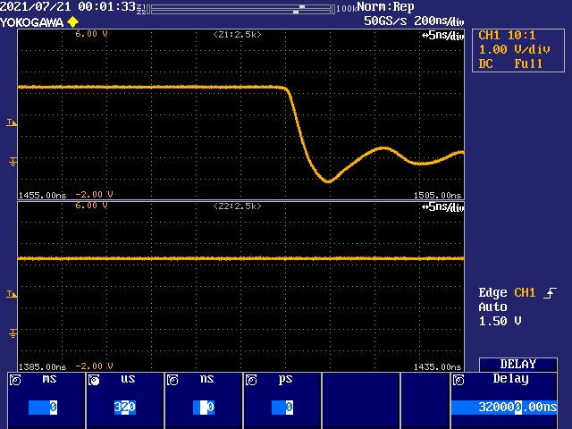
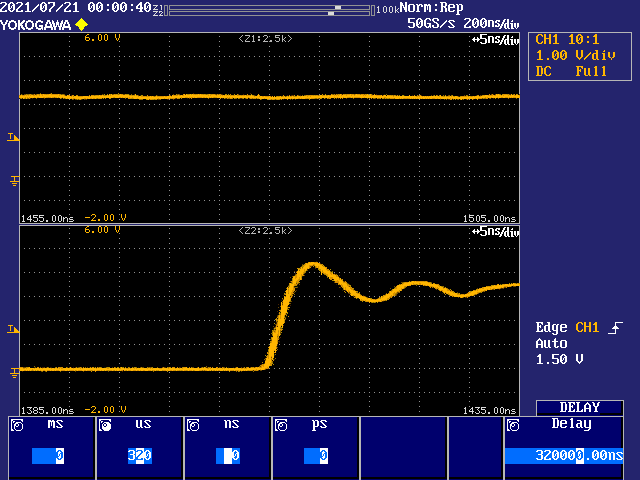
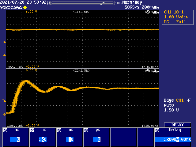
Actually the information of evanh's scope trace makes it look like the P2 jitter is only 1ns after a delayed trigger of 320us, (possibly minus 1385ns, I can't quite tell how his scope presents things). If this is indeed the case, 1 part in 320000 is tiny.
I may be wrong, but, along the four sample screens, with the horizontal resolution of the instrument set at 5 nS/Div, I concluded that the "thickness" of the leading/falling ramping of the signal shows the captured information of interest about the amount of jitter, which seems to stand for ~1 nS, @ DIVD = 62.
@Cluso99 said:
Evan, what are you scoping?
The rise time is 200ns and the ringing only drops to about 2V3 to 3V between pics. Am I seeing this correctly?
It's a 1 MHz, or near as, P_NCO_FREQ smartpin. Traces are visually about 2 ns rise and fall times but in reality the pin signals may well be a lot sharper. The analogue frontend of the scope is only 200 MHz so the visible edge slew rates are likely limited more by that. Others here, with wider band scopes and active probes, may be able to show how sharp the edges really are.
Yep, ringing is exceeding 4 volts and dipping under 3 volts on a rise, and fall is going below -1 volt and above 0.5 volt. Again, these are muffled by the scope's limitations.
@rogloh said:
Actually the information of evanh's scope trace makes it look like the P2 jitter is only 1ns after a delayed trigger of 320us, (possibly minus 1385ns, I can't quite tell how his scope presents things). If this is indeed the case, 1 part in 320000 is tiny.
Yep, that's all correct. First time I've played with the delay feature. I've always relied on the deep memory previously. But the jitter doesn't seem to grow proportionally to delay so spec'ing it as parts-per-million doesn't work, this simply at least. 320 μs is just where I'd left it, 20 μs looks the same.
@Yanomani said:
I may be wrong, but, along the four sample screens, with the horizontal resolution of the instrument set at 5 nS/Div, I concluded that the "thickness" of the leading/falling ramping of the signal shows the captured information of interest about the amount of jitter, which seems to stand for ~1 nS, @ DIVD = 62.
I turned on persistence display mode, with 5 second fade, to help make the thickness more solid. Sitting down and tinkering beats the Smile out of reading the manual.
Oh, the 200 ns/div value displayed up the top of the screenshots is for the unzoomed full capture, 100,000 samples per trace. That particular display is zoomed into two consecutive locations, with the lower window just ahead of the upper window. You can see the two little Z1 and Z2 bars at the top. The positions and zoom widths within the full capture buffer are indicated with the white blocks.
@evanh said:
320 μs is just where I'd left it, 20 μs looks the same.
Thanks, I was thinking to ask you if it was the same jitter much closer in. Seems it is.
Intriguing, I don't understand the mechanics of this but after some more testing of delayed triggering, it looks like the effect of delay on the thickness of the jitter fuzz also depends on the actual jitter amount that's present, ie: A small jitter case can only be visually amplified by a small delay. Applying more delay has no further effect. Vis-a-vis, with a signal that is clearly less stable from the base 1.5 μs (zoomed position), a lot more delay can be applied and have the thickness increased even more.
Okay, it's some natural modulation. I haven't tried to sort out the parameters but the jitter phases in and out at some lower frequency for each given mode, something like 50 kHz to 1 MHz range. So no fixed trigger delay works for all modes. Larger is no guarantee of covering it. I'm not sure how to define the amount of jitter for a given mode now.
Here's a new display mode, called accumulate, that in this case gives the trace in the lower window a 3D look. But looking at the upper window, unzoomed, it also demonstrates the phasing of the jitter as it gets thicker in the middle but thins out again on either side:
PS: Don't freak about this example. I'm way outside the permitted limits again with the VCO down at 20.67 MHz.
Simply amazing how it agrees with expected statistical results.
Ellaborating a bit: with VCO @20.67 MHz, each one of its seven stages would be responsible for ~6.9 nS of delay, thus + - 1 stage would give (2 x 6.9) = 13.8 nS (zoom at 10 nS/div), which is the total jitter we are seeing at the image. Fantastic!
P2 VCO is composed by seven delay stages in series, so, e.g., when the VCO is running at 20.67 MHz, each of its cycles lasts 48.38 nS, thus each delay stage is responsible for 48.38 / 7 = 6.91 nS.
The PFD is responsible for the commanding of the bias voltage generator that, in its turn, controls the amount of delay of each and every stage.
It exerts this control by means of a single bit, so the bias can only increase or decrease, but not kept steady.
The net result of this arrangement is that the VCO frequency is ever varying, increasing, or decreasing, within the limits of +- one of its stages delays.
P.S. Just ignore the above part; there are clearly two bits, DOWN and UP, so, when both are in their inactive state, the bias generator will try to keep stable, and so does the delay of each stage.
Then, the resulting frequency will tend to stabilize, pending further variations at the reference input, or bias source.
The maximum span the difference between both periods can grow, in each direction, is limited to one elemental delay, before being corrected by a change in the DONW/UP controls.
Since the image you've posted above is the superposition of many instances, yelding around the (imaginary) center point of zero difference (or zero jitter), the horizontal limit should be within +- one unity delay of the cycle, which it does, indeed.
P. S. Naturally, any eventual variation introduced by the input reference frequency, being it due either crystal or clock oscillator jitter, is included into the image too.(Redundant)
P.S. II : There is a better and more complete explanation at post #361, just ahead, with an example image.
At the example images you posted before, the waveforms seems to be affected by some over/undershot.
Perhaps part of those distortions could be attributed to some artifacts introduced by the bandwhidth-limited input of the scope (in that case, 200 MHz, IIRC).
@Yanomani said:
... the horizontal limit should be within +- one unity delay of the cycle, which it does, indeed.
Ah, and the other detail is the continuous variability of the stages. I hadn't imagined this but, in hindsight, I see it wouldn't be finely tunable otherwise.
It's the way P2 VCO is designed: seven inverting delay elements (or stages), chained in series. The last stage output (which is the one who drives the VCO output) is also fed to the chain input, forming a ring.
Since seven is odd, they act, in fact, as a single inverter, whose total delay is the sum of each one of its constituting parts.
But, as each half cycle of VCO's waveform must pass thru the whole chain, before being fed back to the input, each complete cycle comprises a total of 14 (fourteen) individual delays.
And there resides a gross mistake I did before, at post #357, when I asserted that each stage is responsible for ~6.91 nS, without explaining that, in fact, the real value should be ~3.45 nS per stage, BUT, only a half cycle of the VCO waveform travels thru the ring, each time.
Thus, the complete waveform takes twice the time to completelly traverse the ring, or 14 x 3.45 nS.
I should have used 20.67 MHz * 2 = 41.34 MHz in my calculations, leading to an individual delay of ~3.45 nS per stage, and also should have done a more "visual" explanation, as a waveform plot, which I did now (.png image appended).
Naturally, each stage is responsible for ~6.91 nS of delay; 3.45 nS during the "high" half of each cycle, and another 3.45 nS during the "low" half.
The maximum span each of the small variations can pile up or down, till a change at the bias generator is commanded by the PFD, can still ammount to 6.91 nS (in each direction), as depicted at the image you've appended to post #354.
Sorry about my mistake, and any confusion it could be cause of.


Comments
Oh man. What sort of crystal + frequency combo runs out of multiplier with values up to 1024? Are you using 32768Hz crystals or something?
Also, @evanh, I've modified the routine below that determines the PLL parameters to try to use your suggestion... am testing further but it still seems to work.
MAXCLK_HZ is now set to 350000000
MAXVCO_HZ is now set to 250000000 (if I set only to 200MHz, it would fail to allow certain integer MHz frequencies).
PRI computeClockMode(desiredHz) : mode | vco, finput, fr, p, div, m, error, bestError bestError := -1 repeat p from 0 to 30 step 2 ' compute the ideal VCO frequency fr at this value of P if p <> 0 if desiredHz > MAXVCO_HZ/p ' test it like this to not overflow quit fr := desiredHz * p else fr := desiredHz if fr > MAXCLK_HZ quit ' scan through D values, and find best M, retain best case repeat div from 1 to 64 'compute the PLL input frequency from the crystal through the divider finput := xtal/div if finput < MINPLLIN_HZ ' input getting too low, and only gets lower so quit now quit ' determine M value needed for this ideal VCO frequency and input frequency m := fr / finput ' send("trying p=",f.unsdec(p), " d=", f.unsdec(div), " m=", f.unsdec(m),13,10) ' check for the out of divider range case if m +> 1024 quit ' zero is special and gets a second chance if m == 0 m++ ' compute the actual VCO frequency at this particular M, D setting vco := finput * m if vco +< MINVCO_HZ next if vco +> MAXCLK_HZ next ' compute the error and check next higher M value if possible, it may be closer error := abs(fr - vco) if m < 1024 and (vco + finput) +< MAXCLK_HZ if error > abs(fr - (vco + finput)) error := abs(fr - (vco + finput)) m++ ' retain best allowed frequency error and divider bits found so far if error +< bestError and error +< TOLERANCE_HZ+1 bestError := error mode := ((div-1) << 18) + ((m-1) << 8) + (((p/2 - 1) & $f) << 4) mode |= (1<<24) ' enable PLL ' quit whenever perfect match found if bestError == 0 quit if bestError == 0 quit ' final clock mode format is this #%0000_000E_DDDD_DDMM_MMMM_MMMM_PPPP_CCSS if mode ' also set 15 or 30pF capacitor loading based on input crystal frequency if (CLKSRC == CLKSRC_XTAL) ' enable oscillator and caps for crystal mode |= (xtal < 16000000) ? %1111 : %1011 else mode |= %0111 ' don't enable oscillatorRegular 20 MHz, it's all in the algo trying to find best fit at 100 kHz increments.
Jitter is stable for everything I monitored in that list. Mostly the beginning. It was stepping increments per 1.2 seconds so took a while. I actually went and watched some telly before 20 MHz sysclock. But had also been watching many other runs before that.
To prove it, in another run, I temporarily allowed poor jitter by dropping the minimum Fvco limit to 30 MHz and did indeed get visible jitter on the scope.
It's in C. Here's the current source (Roughly based on Chip's code):
static uint32_t pll_calc( uint32_t targetfreq ) // returns a suitable _clkset() mode value, or 0 for an out-of-bounds result { enum { _MINFPFD = 250, // units are kHz _XTLFRQ = (_XTALFREQ+500)/1000, // units are kHz }; int32_t mult, divd, divp, post, Fpfd, Fvco, error, besterror = _MINFPFD; uint32_t mode = 0; targetfreq = MAX( (targetfreq + 500) / 1000, 1 ); // convert to units of kHz for( post = 15; post >= 0; post-- ) { divp = post ? post * 2 : 1; for( divd = 1; divd <= 64; divd++ ) { Fpfd = (_XTLFRQ + (divd>>1)) / divd; // units are kHz mult = ((int32_t)targetfreq * divp * divd + _XTLFRQ/2) / _XTLFRQ; Fvco = (_XTLFRQ * mult + (divd>>1)) / divd; // units are kHz if( (Fpfd >= _MINFPFD) && (mult <= 1024) && (Fvco >= 99900) && ((Fvco <= 201000) || (Fvco <= (int32_t)targetfreq + _MINFPFD)) ) { error = (Fvco + (divp>>1)) / divp - targetfreq; // units are kHz error = abs( error ); if( error < besterror ) { mode = 1<<24 | (divd-1)<<18 | (mult-1)<<8 | ((post-1)&0x0f)<<4 | 0x0b; // %CC==%10 %SS==11 besterror = error; } } } } return mode; }Yeah that would take quite a while.
Ha, woke up this morning with the realisation I should make and use a muldiv65() - https://forums.parallax.com/discussion/comment/1525687/#Comment_1525687
It'll get rid of a bunch of ugliness in my code above.
Much better! Using the 64-bit intermediate allows unit resolution of Hz instead of the prior kHz. It should now be very close to exact match of Chip's results with floats.
static uint32_t  div33( uint32_t dividend, uint32_t divisor )
{
    uint32_t  x;

    __asm {
        mov x, divisor
        shr x, #1
        add dividend, x
        qdiv    dividend, divisor
        getqx   x
    }

    return  x;
}


static uint32_t  muldiv65( uint32_t mult1, uint32_t mult2, uint32_t divisor )
{
    uint32_t  x;

    __asm {
        qmul    mult1, mult2
        mov x, divisor
        shr x, #1
        getqx   mult1
        getqy   mult2
        add mult1, x    wc
        addx    mult2, #0
        setq    mult2
        qdiv    mult1, divisor
        getqx   x
    }

    return  x;
}


static uint32_t  mul2div65( uint16_t mult1, uint16_t mult2, uint32_t mult32, uint32_t divisor )
{
    uint32_t  x;

    __asm {
        mul mult1, mult2
        mov x, mult1
    }

    return  muldiv65( x, mult32, divisor );
}


static uint32_t  pll_calc( uint32_t targetfreq )  // returns a suitable _clkset() mode value, or 0 for an out-of-bounds result
{
    enum {
        _MINFPFD = 250_000,
    };
    uint32_t  mult, divd, divp, post, Fpfd, Fvco, mode = 0;
    int32_t  error, besterror = _MINFPFD;

    for( post = 0; post <= 15; post++ )
    {
        divp = post ? post * 2 : 1;
        for( divd = 64; divd >= 1; divd-- )
        {
            mult = mul2div65( divp, divd, targetfreq, _XTALFREQ );
            Fvco = muldiv65( _XTALFREQ, mult, divd );
            Fpfd = div33( _XTALFREQ, divd );

            if( (Fpfd >= _MINFPFD)
                && (mult <= 1024)
                && (Fvco >= 100_000_000)
                && ((Fvco <= 201_000_000) || (Fvco <= targetfreq + _MINFPFD)) )
            {
                error = abs( (int32_t)(div33( Fvco, divp ) - targetfreq) );
                if( error <= besterror )
                {
                    mode = 1<<24 | (divd-1)<<18 | (mult-1)<<8 | ((post-1)&0x0f)<<4 | 0x0b;  // %CC==%10 %SS==11
                    besterror = error;
                }
            }
        }
    }

    return  mode;
}
EDIT: Removed some redundant code.
There is a particular order that Chip devised that assigns priority of component selection when there is more than one solution. The downside is it demands iterating the full set.
I came to terms with its importance about half way through my bug fixes. Most of my effort went into accuracy and de-glitching the corner cases ... but as I cleared those away it became apparent there was still poor selection of component values in some cases. And of course I had put in my own subtle deviation on Chip's solution at that time.
Where Chip has the sequence of incrementing divp and decrementing divd, I had those flipped. It didn't seem significant at first glance because all combinations get tested anyway. However, the accept/reject test in Chip's algorithm uses
(e <= error). The equality portion has big impact particularly on a zero error. It means it will keep accepting new zero-errors as they get found. Which in turn means that the final zero-error is the one chosen!So, because I had reversed the search order but the same result is still desired the accept/reject condition also needed a tweak, namely
( error < besterror ). The equality portion is removed, therefore the first zero-error gets chosen. This then gives same outcome as Chip's algorithm.In the second listing above I flipped it back to same order as Chip's algorithm because I'd elected to use unsigned integers which posed an issue for termination of the first for-loop in my first algorithm.
@evanh In practice how much worse is the case with a higher p value or different m/d if the error is the same? Are you seeing a lot of PLL jitter differences over the ranges of values you tested?
Higher DIVP is better. It allows reduction of DIVD, which is preferable for avoiding jitter cases. So far, I haven't seen any problems, but then I didn't hook up the scope till late in the cleanup.
I'll flip the priorities now and check ...
Hmm, the DIVP part only really affects very low target frequencies. But what does happen, for my algorithm, is DIVD priority is reversed and that definitely has an impact. Here's a good case:
And the equivalent bad case:
Although, bad isn't really bad at all. Jitter isn't really all that different except for the cases where DIVD is below 10 maybe. Then the jitter is much lower.
Examples:
DIVD = 1
DIVD = 5

DIVD = 8
DIVD = 62
Ok, well you can definitely see the jitter go up as DIVD increases. Still remains under ~1ns up to DIVD of 62. 1ns of jitter on the IO is probably going to make those HyperRAM accesses at high clock speeds a little more marginal though around the transitions.
Evan, what are you scoping?
The rise time is 200ns and the ringing only drops to about 2V3 to 3V between pics. Am I seeing this correctly?
Actually the information of evanh's scope trace makes it look like the P2 jitter is only 1ns after a delayed trigger of 320us, (possibly minus 1385ns, I can't quite tell how his scope presents things). If this is indeed the case, 1 part in 320000 is tiny.
I may be wrong, but, along the four sample screens, with the horizontal resolution of the instrument set at 5 nS/Div, I concluded that the "thickness" of the leading/falling ramping of the signal shows the captured information of interest about the amount of jitter, which seems to stand for ~1 nS, @ DIVD = 62.
It's a 1 MHz, or near as, P_NCO_FREQ smartpin. Traces are visually about 2 ns rise and fall times but in reality the pin signals may well be a lot sharper. The analogue frontend of the scope is only 200 MHz so the visible edge slew rates are likely limited more by that. Others here, with wider band scopes and active probes, may be able to show how sharp the edges really are.
Yep, ringing is exceeding 4 volts and dipping under 3 volts on a rise, and fall is going below -1 volt and above 0.5 volt. Again, these are muffled by the scope's limitations.
Yep, that's all correct. First time I've played with the delay feature. I've always relied on the deep memory previously. But the jitter doesn't seem to grow proportionally to delay so spec'ing it as parts-per-million doesn't work, this simply at least. 320 μs is just where I'd left it, 20 μs looks the same.
I turned on persistence display mode, with 5 second fade, to help make the thickness more solid. Sitting down and tinkering beats the Smile out of reading the manual.")
Oh, the 200 ns/div value displayed up the top of the screenshots is for the unzoomed full capture, 100,000 samples per trace. That particular display is zoomed into two consecutive locations, with the lower window just ahead of the upper window. You can see the two little Z1 and Z2 bars at the top. The positions and zoom widths within the full capture buffer are indicated with the white blocks.
I missed the 5ns/div. Just saw the 200ns/div
Thanks, I was thinking to ask you if it was the same jitter much closer in. Seems it is.
Intriguing, I don't understand the mechanics of this but after some more testing of delayed triggering, it looks like the effect of delay on the thickness of the jitter fuzz also depends on the actual jitter amount that's present, ie: A small jitter case can only be visually amplified by a small delay. Applying more delay has no further effect. Vis-a-vis, with a signal that is clearly less stable from the base 1.5 μs (zoomed position), a lot more delay can be applied and have the thickness increased even more.
I need to devise an exhaustive test ...
Okay, it's some natural modulation. I haven't tried to sort out the parameters but the jitter phases in and out at some lower frequency for each given mode, something like 50 kHz to 1 MHz range. So no fixed trigger delay works for all modes. Larger is no guarantee of covering it. I'm not sure how to define the amount of jitter for a given mode now.
Here's a new display mode, called accumulate, that in this case gives the trace in the lower window a 3D look. But looking at the upper window, unzoomed, it also demonstrates the phasing of the jitter as it gets thicker in the middle but thins out again on either side:
PS: Don't freak about this example. I'm way outside the permitted limits again with the VCO down at 20.67 MHz.
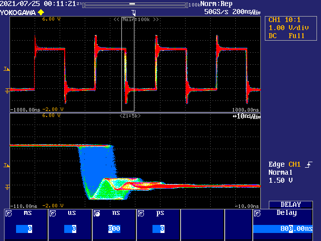
Simply amazing how it agrees with expected statistical results.
Ellaborating a bit: with VCO @20.67 MHz, each one of its seven stages would be responsible for ~6.9 nS of delay, thus + - 1 stage would give (2 x 6.9) = 13.8 nS (zoom at 10 nS/div), which is the total jitter we are seeing at the image. Fantastic!
More elaboration please. What is a stage? I'm guessing a logic inverter. Why only two in above example?
P2 VCO is composed by seven delay stages in series, so, e.g., when the VCO is running at 20.67 MHz, each of its cycles lasts 48.38 nS, thus each delay stage is responsible for 48.38 / 7 = 6.91 nS.
The PFD is responsible for the commanding of the bias voltage generator that, in its turn, controls the amount of delay of each and every stage.
It exerts this control by means of a single bit, so the bias can only increase or decrease, but not kept steady.
The net result of this arrangement is that the VCO frequency is ever varying, increasing, or decreasing, within the limits of +- one of its stages delays.
P.S. Just ignore the above part; there are clearly two bits, DOWN and UP, so, when both are in their inactive state, the bias generator will try to keep stable, and so does the delay of each stage.
Then, the resulting frequency will tend to stabilize, pending further variations at the reference input, or bias source.
The maximum span the difference between both periods can grow, in each direction, is limited to one elemental delay, before being corrected by a change in the DONW/UP controls.
Since the image you've posted above is the superposition of many instances, yelding around the (imaginary) center point of zero difference (or zero jitter), the horizontal limit should be within +- one unity delay of the cycle, which it does, indeed.
P. S. Naturally, any eventual variation introduced by the input reference frequency, being it due either crystal or clock oscillator jitter, is included into the image too. (Redundant)
P.S. II : There is a better and more complete explanation at post #361, just ahead, with an example image.
For reference only (credits to Intel):
https://intel.cn/content/www/cn/zh/programmable/support/support-resources/operation-and-testing/pll-and-clock-management/pll-basics.html
Hi evanh,
At the example images you posted before, the waveforms seems to be affected by some over/undershot.
Perhaps part of those distortions could be attributed to some artifacts introduced by the bandwhidth-limited input of the scope (in that case, 200 MHz, IIRC).
https://signalintegrityjournal.com/articles/2175-how-to-avoid-gibbs-ringing-artifacts-in-measurements
If that's the case, perhaps adjusting the strength of P2 output drivers can help alleviating the someway confusing visual effects.
The slew rate would be affected, but, as explainned at the article, the jitter will not.
Hope it helps.
Henrique
I ignore the voltage overshoot. Doesn't worry me.
Oh, just noticed your main point:
Ah, and the other detail is the continuous variability of the stages. I hadn't imagined this but, in hindsight, I see it wouldn't be finely tunable otherwise.
Next question: Why have seven stages?
It's the way P2 VCO is designed: seven inverting delay elements (or stages), chained in series. The last stage output (which is the one who drives the VCO output) is also fed to the chain input, forming a ring.
Since seven is odd, they act, in fact, as a single inverter, whose total delay is the sum of each one of its constituting parts.
But, as each half cycle of VCO's waveform must pass thru the whole chain, before being fed back to the input, each complete cycle comprises a total of 14 (fourteen) individual delays.
And there resides a gross mistake I did before, at post #357, when I asserted that each stage is responsible for ~6.91 nS, without explaining that, in fact, the real value should be ~3.45 nS per stage, BUT, only a half cycle of the VCO waveform travels thru the ring, each time.
Thus, the complete waveform takes twice the time to completelly traverse the ring, or 14 x 3.45 nS.
I should have used 20.67 MHz * 2 = 41.34 MHz in my calculations, leading to an individual delay of ~3.45 nS per stage, and also should have done a more "visual" explanation, as a waveform plot, which I did now (.png image appended).
Naturally, each stage is responsible for ~6.91 nS of delay; 3.45 nS during the "high" half of each cycle, and another 3.45 nS during the "low" half.
The maximum span each of the small variations can pile up or down, till a change at the bias generator is commanded by the PFD, can still ammount to 6.91 nS (in each direction), as depicted at the image you've appended to post #354.
Sorry about my mistake, and any confusion it could be cause of.