I know: On the very left where it says even pins 0,2,4,...62, that could be written as even pins P0,P2,P4,...P62.
And the text in the pin block could have "I/O" added: ie: Physical Even # I/O Pin
EDIT: Maybe "Physical" can just be removed. The emphasis was intended to convey that's the off-chip connection point but it's probably overkill really.
@sjgallagher2 speaking with Chip this morning, we'd like to adopt your starting efforts as the foundation for the Propeller 2 datasheet.
I'm going to contact you via PM - my e-mail is kgracey@parallax.com.
Thanks,
Ken Gracey
@"Ken Gracey" said:
@sjgallagher2 speaking with Chip this morning, we'd like to adopt your starting efforts as the foundation for the Propeller 2 datasheet.
I'm going to contact you via PM - my e-mail is kgracey@parallax.com.
Thanks,
Ken Gracey
Hey I've had to take time off from P2 stuff the last few months. But I did catch the May 6 live forum, and noticed there was no mention of this work! I'm happy to see other documentation is getting done, but I think the work I've done here is far ahead of the 'official' docs, and should get a mention. Did anything ever come about from your adoption idea? Much interested to know! Thanks for all your guys work
PS. Let me know if there's anything I can do to help out! I tried to leave things in a good format so they're easy to pick up, and I might not have as much time, but I'm always available if you have questions and always happy to help. I'm loving the content in the new docs too.
So sorry for the absence of mention! You're entirely right that we should've attributed your document as a starting point. Our Editor, Stephanie, is consolidating content from several sources including yours. The source control is now internal at Parallax so we can manage things a bit more quickly.
Over the last few days, I made low-level smart pin schematics to show what you get in each different mode. These are configured by the %PPPPPPPPPPPPP bits outlined in the silicon doc here:
Good one Chip. This helps show how versatile the Smartpin IO pad modes can be. Nice to have these pictures to help understand the capabilities visually. The old table format was always somewhat of a challenge to decipher from scratch on its own.
Now we need app notes for building things around these functions.
The two-pin unclocked feedback modes are continuous in operation and can be used to close control loops. The clocked modes can do the same, but they also give you quantization data.
@evanh said:
Nooo! Naming that a smartpin muddies things. That's just configurable I/O. Leave the smartpin naming with the %MMMMM selectable state machine.
PS: I do like the diagrams a lot, BTW. Showing the output in front of the input is brilliant introduction for perception.
All right I will not call them low-level smart pins, but configurable I/Os.
Not within the pad-ring. The source select and gain is listed top right. The sigma-delta ADC produces a PDM (Pulse Density Modulation) bitstream to IN input. PCM (Pulse Code Modulation) translation is performed deeper in, namely in the smartpin via Sinc filtering and decimation.
@evanh said:
Nooo! Naming that a smartpin muddies things. That's just configurable I/O. Leave the smartpin naming with the %MMMMM selectable state machine.
PS: I do like the diagrams a lot, BTW. Showing the output in front of the input is brilliant introduction for perception.
Thanks, Evanh. I got the language all straightened out now. I also added your edits to the 27-bit accumulator issue for the SINC2/SINC3 modes. Could you please check if it reads okay now?
@cgracey said:
I updated the main pin diagram to spell out 64 instances, plus I consolidated the level-comparator modes with separate feedback.
Oh, make the Adjacent Pin shaded or dotted outline. That'll clarify that the adjacent pin has it's own instance. The ill-defined pin duplication had bothered me when doing the block diagram too.
@cgracey said:
Thanks, Evanh. I got the language all straightened out now. I also added your edits to the 27-bit accumulator issue for the SINC2/SINC3 modes. Could you please check if it reads okay now?
Not within the pad-ring. The source select and gain is listed top right. The sigma-delta ADC produces a PDM (Pulse Density Modulation) bitstream to IN input. PCM (Pulse Code Modulation) translation is performed deeper in, namely in the smartpin via Sinc filtering and decimation.
Then should there be a dotted box connecteD to the input pin suggesting the smart pin options?
We want people to understand there is much more than these basic modes too. These are the blocks that will help sell the P2, so we don’t want to miss anything important here.
@Cluso99 said:
Is the adjacent pin the next pin (ie +1) or +/-3?
No, different area of the chip, this is all entirely within the pad-ring. They're an odd/even set pair, just like the partner Cog for lutRAM sharing. Maybe "partner" would be better name than "adjacent". Whereas the %AAAA_BBBB input selects in front of the smartpin are straight relative to that pin.
Not within the pad-ring. The source select and gain is listed top right. The sigma-delta ADC produces a PDM (Pulse Density Modulation) bitstream to IN input. PCM (Pulse Code Modulation) translation is performed deeper in, namely in the smartpin via Sinc filtering and decimation.
Then should there be a dotted box connecteD to the input pin suggesting the smart pin options?
We want people to understand there is much more than these basic modes too. These are the blocks that will help sell the P2, so we don’t want to miss anything important here.
Maybe a note to say IN is a bitstream for a smartpin to capture. Doesn't have to be that pin's smartpin either. But the smartpin modes should stay listed independently of this. Each mode needs a lot of explaining and will be a large section of the finished manual.
@cgracey said:
Thanks, Evanh. I got the language all straightened out now. I also added your edits to the 27-bit accumulator issue for the SINC2/SINC3 modes. Could you please check if it reads okay now?
Chip,
There is a disjointedness between the ENOB calculation and my assertion of 27 bits. They should be combined. Say something like ENOB shift and mask must be within the bounds of the 27-bit accumulator width.
@Cluso99 said:
Is the adjacent pin the next pin (ie +1) or +/-3?
No, different area of the chip, this is all entirely within the pad-ring. They're an odd/even set pair, just like the partner Cog for lutRAM sharing. Maybe "partner" would be better name than "adjacent". Whereas the %AAAA_BBBB input selects in front of the smartpin are straight relative to that pin.
Thanks Evan. As you can probably tell, I haven't done anything with smartpins or the config i/o other than to use pullups/pulldowns and uarts.
I am amazed at the various functions available here!
@cgracey said:
I updated the main pin diagram to spell out 64 instances, plus I consolidated the level-comparator modes with separate feedback.
Chip,
There's a recurring error in all the clocked sdac compare cases - The flip-flop should be just in front of OE buffer. And feedback/IN should be prior to the flip-flop.
Also, the inverter and non-inverter cases of the same compare group can be merged same as you've done elsewhere. Oh, maybe not. I see there is an encoding limitation there.
@cgracey said:
Thanks, Evanh. I got the language all straightened out now. I also added your edits to the 27-bit accumulator issue for the SINC2/SINC3 modes. Could you please check if it reads okay now?
Chip,
There is a disjointedness between the ENOB calculation and my assertion of 27 bits. They should be combined. Say something like ENOB shift and mask must be within the bounds of the 27-bit accumulator width.


Comments
I know: On the very left where it says even pins 0,2,4,...62, that could be written as even pins P0,P2,P4,...P62.
And the text in the pin block could have "I/O" added: ie: Physical Even # I/O Pin
EDIT: Maybe "Physical" can just be removed. The emphasis was intended to convey that's the off-chip connection point but it's probably overkill really.
+1
@sjgallagher2 speaking with Chip this morning, we'd like to adopt your starting efforts as the foundation for the Propeller 2 datasheet.
I'm going to contact you via PM - my e-mail is kgracey@parallax.com.
Thanks,
Ken Gracey
Hey I've had to take time off from P2 stuff the last few months. But I did catch the May 6 live forum, and noticed there was no mention of this work! I'm happy to see other documentation is getting done, but I think the work I've done here is far ahead of the 'official' docs, and should get a mention. Did anything ever come about from your adoption idea? Much interested to know! Thanks for all your guys work
PS. Let me know if there's anything I can do to help out! I tried to leave things in a good format so they're easy to pick up, and I might not have as much time, but I'm always available if you have questions and always happy to help. I'm loving the content in the new docs too.
So sorry for the absence of mention! You're entirely right that we should've attributed your document as a starting point. Our Editor, Stephanie, is consolidating content from several sources including yours. The source control is now internal at Parallax so we can manage things a bit more quickly.
Thank you for your contribution @sjgallagher2.
Ken Gracey
Over the last few days, I made low-level smart pin schematics to show what you get in each different mode. These are configured by the %PPPPPPPPPPPPP bits outlined in the silicon doc here:
https://docs.google.com/document/d/1gn6oaT5Ib7CytvlZHacmrSbVBJsD9t_-kmvjd7nUR6o/edit?usp=sharing
I added them all into the doc just now.
Note that the %PPPPPPPPPPPPP bits were renamed to %BBBBBBBBBBBBB so as not to confuse them with pins P0..P12.
Here they are:
Good one Chip. This helps show how versatile the Smartpin IO pad modes can be. Nice to have these pictures to help understand the capabilities visually. The old table format was always somewhat of a challenge to decipher from scratch on its own.
Now we need app notes for building things around these functions.
The two-pin unclocked feedback modes are continuous in operation and can be used to close control loops. The clocked modes can do the same, but they also give you quantization data.
Nooo! Naming that a smartpin muddies things. That's just configurable I/O. Leave the smartpin naming with the %MMMMM selectable state machine.
PS: I do like the diagrams a lot, BTW. Showing the output in front of the input is brilliant introduction for perception.
All right I will not call them low-level smart pins, but configurable I/Os.
Nicely done Chip
I agree with Evan that these functions should be called configurable I/O and keep the smartpins for the state machine.
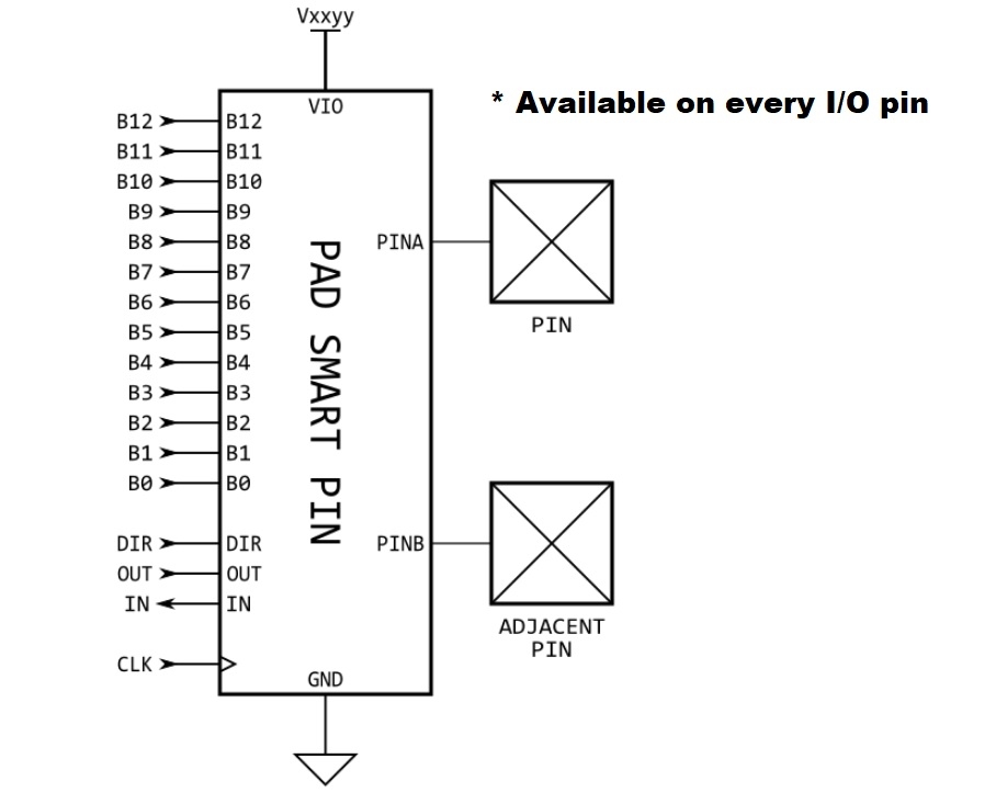
I suggest on the first block diagram, on the RHS, make a big point that these are available on every I/O pin
Also a question
Is the adjacent pin selectable +/-3 pins? If so, also add this statement to the adjacent pin pic here.
IMHO we also need a section here showing how the inbuilt DACs add into this.
Are there other ADC modes?
Maybe Configurable I/O plus DAC and ADC ???
This is so when these are seen, they note that there are still other modes too.
And a note that there are also SmartPins modes too (see other docs)
Thanks Chip!
The many ways configurable I/Os (Thanks to evanh, too!) can get rearranged are very clear now. Amazing work...
Not within the pad-ring. The source select and gain is listed top right. The sigma-delta ADC produces a PDM (Pulse Density Modulation) bitstream to IN input. PCM (Pulse Code Modulation) translation is performed deeper in, namely in the smartpin via Sinc filtering and decimation.
Just noticed this on P7 in the datasheet linked above
8-deep stack for subroutine call return address + flags or data (32 bits wide)
This sounds limiting so perhaps there should be something that explains external stack space in registers/hub is also available.
I changed it to this:
8-level hardware stack for fastest subroutine calls/returns and push/pop operations
I updated the main pin diagram to spell out 64 instances, plus I consolidated the level-comparator modes with separate feedback.
Thanks, Evanh. I got the language all straightened out now. I also added your edits to the 27-bit accumulator issue for the SINC2/SINC3 modes. Could you please check if it reads okay now?
Oh, make the Adjacent Pin shaded or dotted outline. That'll clarify that the adjacent pin has it's own instance. The ill-defined pin duplication had bothered me when doing the block diagram too.
Updated info: Saucy pointed out that analogue input saturation generates overflow in the Sinc3 accumulators when set to period of 512 bit-clocks - https://forums.parallax.com/discussion/comment/1523646/#Comment_1523646
Off to work now. I'll read more later.
Then should there be a dotted box connecteD to the input pin suggesting the smart pin options?
We want people to understand there is much more than these basic modes too. These are the blocks that will help sell the P2, so we don’t want to miss anything important here.
I wonder if the first diagram here should have the dotted smart pin box added too?
Is the adjacent pin the next pin (ie +1) or +/-3?
No, different area of the chip, this is all entirely within the pad-ring. They're an odd/even set pair, just like the partner Cog for lutRAM sharing. Maybe "partner" would be better name than "adjacent". Whereas the %AAAA_BBBB input selects in front of the smartpin are straight relative to that pin.
Maybe a note to say IN is a bitstream for a smartpin to capture. Doesn't have to be that pin's smartpin either. But the smartpin modes should stay listed independently of this. Each mode needs a lot of explaining and will be a large section of the finished manual.
Chip,
There is a disjointedness between the ENOB calculation and my assertion of 27 bits. They should be combined. Say something like ENOB shift and mask must be within the bounds of the 27-bit accumulator width.
Thanks Evan. As you can probably tell, I haven't done anything with smartpins or the config i/o other than to use pullups/pulldowns and uarts.
I am amazed at the various functions available here!
Chip,
The new "B" bit-field naming kind of conflicts with the existing %BBBB input select. How about "C"? Short for custom pad-ring.
Chip,
There's a recurring error in all the clocked sdac compare cases - The flip-flop should be just in front of OE buffer. And feedback/IN should be prior to the flip-flop.
Also, the inverter and non-inverter cases of the same compare group can be merged same as you've done elsewhere. Oh, maybe not. I see there is an encoding limitation there.
Oh, okay, I think I see what you've done. You've hidden the signal path duplication of two actual parallel flops.
Yes, and tricky about the set inversion too, those mode specific cases again. The DAC data bits take away the other options.
Okay. Thanks, Evan. I will look at it.