@Cluso99 said:
Perhaps you could have placed the vga connector on the add on board instead?
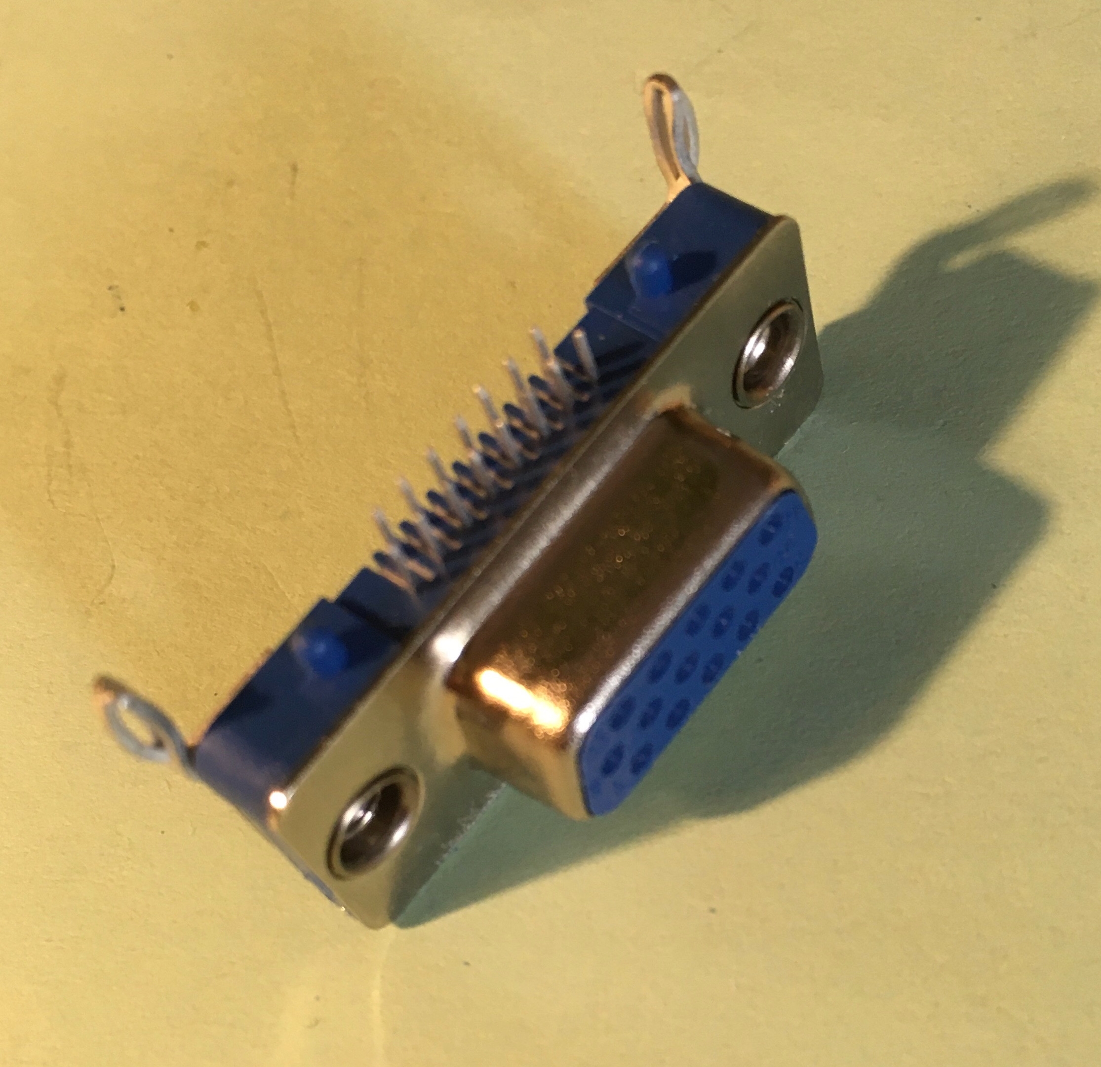
In theory it should be possible, but the board has all 15 vga pins brought out and the traces go from the 16 pin header to the vga connector and then further to the pin header. So quite some fiddling would have been involved and after desoldering the vga connector on the breakout board I didn’t fancy any more of that. However, I had to scrape off half a millimetre of my vga plug to make it fit… so next time I will probably try to modify the breakout board…
@Cluso99 said:
Perhaps you could have placed the vga connector on the add on board instead?
In theory it should be possible, but the board has all 15 vga pins brought out and the traces go from the 16 pin header to the vga connector and then further to the pin header. So quite some fiddling would have been involved and after desoldering the vga connector on the breakout board I didn’t fancy any more of that. However, I had to scrape off half a millimetre of my vga plug to make it fit… so next time I will probably try to modify the breakout board…
That’s a shame
Maybe my next rev (I would still make the existing pcb) should extend the pcb like this?
I’m short on space at the top of the pcb to move the flash onto the front of the pcb, and I’d really like to add a header for the extra P48-57 pins. IMHO P58-61 (Flash/SD) should remain just on the pcb. And I’d like to use the newer CP2102 boards with microUSB - they have an incompatible 5-6pin header
@Cluso99 said:
Maybe my next rev (I would still make the existing pcb) should extend the pcb like this?
I’m short on space at the top of the pcb to move the flash onto the front of the pcb, and I’d really like to add a header for the extra P48-57 pins. IMHO P58-61 (Flash/SD) should remain just on the pcb. And I’d like to use the newer CP2102 boards with microUSB - they have an incompatible 5-6pin header
Yes to all of those, as long as the pins are DIL :-)
Seeing this picture above, makes me think it would be quite neat to have an extended variant of the Retroblade 2 like above with all P2 I/O pins (from 16-31) available down the sides with this VGA socket moved out and an optional RAM situated where the original VGA connector used to be. Something like this perhaps...
P16-P23 - RAM DATA bus
P24 - CLK
P25 - RWDS
P26 - CE
P27 - VSYNC
P28 - HSYNC
P29 - Blue
P30 - Green
P31 - Red
The main concern would be the extended trace lengths from the memory data signals & clock out to the header pins and any reflections it might cause at high speed etc. That would be an issue but if this issue was worked around (suggestions below) it could be a nice variant. Alternatively you could fit 2x SOIC8 pads for PSRAMs instead of HyperRAM and save that RWDS pin. Jumper it to an LED for debug or something useful. This way you let the user decide if they want to solder on their own PSRAMs, since BGA's are such a PITA to solder on later.
Workarounds: pass memory bus pins down to lower PCB layer and use solder jumpers to bridge through to header pins when RAM is not fitted/used. CE pin could be pulled up via a solder jumper too to disable RAM. Not ideal I know but still probably flexible this way. Maybe even having some of those low profile SMD micro dip switches fitted to the bottom board surface if there is extra room there could work out too for this purpose.
EDIT: I forgot that this board doesn't have a switching regulator power capability. Not sure if it would power a RAM chip in addition to the P2 without getting a bit hot at high speeds.
This type of vga connector ( edac 151-1125-ND ) would also save some space maybe just enough for a switching regulator and some psram? Now it’s getting out of hand…
The main concern would be the extended trace lengths from the memory data signals & clock out to the header pins and any reflections it might cause at high speed etc. That would be an issue but if this issue was worked around (suggestions below) it could be a nice variant. Alternatively you could fit 2x SOIC8 pads for PSRAMs instead of HyperRAM and save that RWDS pin. Jumper it to an LED for debug or something useful. This way you let the user decide if they want to solder on their own PSRAMs, since BGA's are such a PITA to solder on later.
Workarounds: pass memory bus pins down to lower PCB layer and use solder jumpers to bridge through to header pins when RAM is not fitted/used. CE pin could be pulled up via a solder jumper too to disable RAM. Not ideal I know but still probably flexible this way. Maybe even having some of those low profile SMD micro dip switches fitted to the bottom board surface if there is extra room there could work out too for this purpose.
Unfortunately that kind of alternative-"stitching-routing" would still compromise signal integrity, due to the presence of the radiating stubs represented by the unused vias tubbings, by themselves.
The same line of thinking would apply to any kind of mechanical switches, whose unbridged parts can be seen as real emmiting/receiving antennas.
Unspelled thruth about stubs: "If you can't cut (trimm), simply don't put."
With signal switching frequencies in the order of a few hundred MHz, the outstanding harmonics (3rd, 5th, eventually 7th) would easily reach the GHz band, thus, wherever possible (and economically acceptable), it's always better to route fast signals thru analog/digital muxes/switches, and terminate any unused paths accordingly.
Sure, proper routing of GND planes and fills would ever apply.
@aaaaaaaargh Those connectors are expensive and there's a big freight component as I don't buy from those sources either. They are a bit flimsy too so you have to be careful. I plug my VGA cable in/out a lot.
@rogloh I'm not up for BGA currently even tho I have a commercial IR oven. The stencil has slight movement and placing the chips by hand is a problem for me now as I'm getting a little shaky. As for making the pins also available, IMHO that's not a good idea. So it probably needs to be a dedicated design tho this is not out of the question - two pcbs. This would probably push the design into switching regs and 4 layers to dissipate extra P2 heat.


Comments
In theory it should be possible, but the board has all 15 vga pins brought out and the traces go from the 16 pin header to the vga connector and then further to the pin header. So quite some fiddling would have been involved and after desoldering the vga connector on the breakout board I didn’t fancy any more of that. However, I had to scrape off half a millimetre of my vga plug to make it fit… so next time I will probably try to modify the breakout board…
That’s a shame
Maybe my next rev (I would still make the existing pcb) should extend the pcb like this?
I’m short on space at the top of the pcb to move the flash onto the front of the pcb, and I’d really like to add a header for the extra P48-57 pins. IMHO P58-61 (Flash/SD) should remain just on the pcb. And I’d like to use the newer CP2102 boards with microUSB - they have an incompatible 5-6pin header
Yes to all of those, as long as the pins are DIL :-)
Seeing this picture above, makes me think it would be quite neat to have an extended variant of the Retroblade 2 like above with all P2 I/O pins (from 16-31) available down the sides with this VGA socket moved out and an optional RAM situated where the original VGA connector used to be. Something like this perhaps...
P16-P23 - RAM DATA bus
P24 - CLK
P25 - RWDS
P26 - CE
P27 - VSYNC
P28 - HSYNC
P29 - Blue
P30 - Green
P31 - Red
The main concern would be the extended trace lengths from the memory data signals & clock out to the header pins and any reflections it might cause at high speed etc. That would be an issue but if this issue was worked around (suggestions below) it could be a nice variant. Alternatively you could fit 2x SOIC8 pads for PSRAMs instead of HyperRAM and save that RWDS pin. Jumper it to an LED for debug or something useful. This way you let the user decide if they want to solder on their own PSRAMs, since BGA's are such a PITA to solder on later.
Workarounds: pass memory bus pins down to lower PCB layer and use solder jumpers to bridge through to header pins when RAM is not fitted/used. CE pin could be pulled up via a solder jumper too to disable RAM. Not ideal I know but still probably flexible this way. Maybe even having some of those low profile SMD micro dip switches fitted to the bottom board surface if there is extra room there could work out too for this purpose.
EDIT: I forgot that this board doesn't have a switching regulator power capability. Not sure if it would power a RAM chip in addition to the P2 without getting a bit hot at high speeds.
This type of vga connector ( edac 151-1125-ND ) would also save some space maybe just enough for a switching regulator and some psram? Now it’s getting out of hand…
Unfortunately that kind of alternative-"stitching-routing" would still compromise signal integrity, due to the presence of the radiating stubs represented by the unused vias tubbings, by themselves.
The same line of thinking would apply to any kind of mechanical switches, whose unbridged parts can be seen as real emmiting/receiving antennas.
Unspelled thruth about stubs: "If you can't cut (trimm), simply don't put."
With signal switching frequencies in the order of a few hundred MHz, the outstanding harmonics (3rd, 5th, eventually 7th) would easily reach the GHz band, thus, wherever possible (and economically acceptable), it's always better to route fast signals thru analog/digital muxes/switches, and terminate any unused paths accordingly.
Sure, proper routing of GND planes and fills would ever apply.
@aaaaaaaargh Those connectors are expensive and there's a big freight component as I don't buy from those sources either. They are a bit flimsy too so you have to be careful. I plug my VGA cable in/out a lot.
@rogloh I'm not up for BGA currently even tho I have a commercial IR oven. The stencil has slight movement and placing the chips by hand is a problem for me now as I'm getting a little shaky. As for making the pins also available, IMHO that's not a good idea. So it probably needs to be a dedicated design tho this is not out of the question - two pcbs. This would probably push the design into switching regs and 4 layers to dissipate extra P2 heat.
[b]Cluso's Z80/CPM emulation[/b]
[i]27 Nov 2021 update[/i] - new thread with latest code (15Jan2021)
[url="https://forums.parallax.com/discussion/174087/clusos-z80-emulation-for-retroblade2-p2/p1"]https://forums.parallax.com/discussion/174087/clusos-z80-emulation-for-retroblade2-p2/p1[/url]
Now uses 8*8MB HDD emulated CPM files.