

P2 PASM compare three levels, without ADC
 pic18f2550
Posts: 400
pic18f2550
Posts: 400
I have one voltage on each of three pins. (A, B & C)
I just want to find out which one is bigger.
The values are unimportant therefore also without ADC.
I guess I have to change the config between the comparisons.
How is the timing?
Does anyone have an example?
A>B = 1
B>C = 1
C>A = 1
Thank you.
Comments
The internal analogue comparators are only between partitioned odd-even pairs. To do what you want directly with the comparators would require six pins. ie: Only one comparator of each pair is used.
PS: There is also a DAC-compare mode you might want to try. But you'd basically be using software to turn that into a successive approximation ADC.
I have already thought about the DAC version.
The response time with reading and comparison must be under 150ns.
Since I need a quick response on the part of the P2 I have to resort to the comparator method.
Well, each comparator output can be registered (clocked) within the pad-ring. That would give you the most precision for synchronous sampling of the compare out.
Compare out can independently, unregistered, also be fed back to the pin logic output drive circuits within the pad-ring, same path as the logic input feedback. Logic drive has its own registration.
I need to hit the sack right now so I have no examples right now sorry.
Have also already in the "Propeller 2 Rev B/C Smart Pin Supplementary Documentation" but can not find anything on the subject.
You don't need smartpins for that. It's just a lowlevel pin configuration. The comparator can compare and odd and an even pin (0 > 1, 2 > 3, and so on), you read the comparator result just like a normal input via INA, INB or pinread().
I think this should work:
  _clkfreq  = 180_000_000

  'uses 6 pins P0..P5
  PINAgB  = 0      'Signal A to P0 and P5
  PINBgC  = 2      'Signal B to P1 and P2
  PINCgA  = 4      'Signal C to P3 and P4

pub main()
  wrpin(PINAgB, P_COMPARE_AB)
  wrpin(PINBgC, P_COMPARE_AB)
  wrpin(PINCgA, P_COMPARE_AB)
  repeat
    debug("A>B:",udec_(pinr(PINAgB)),"  B>C:",udec_(pinr(PINBgC)),"  C>A:",udec_(pinr(PINCgA)))
    waitms(300)
Andy
In PASM it should work like this.
con CLK_FREQ = 256_000_000 '' system freq as a constan _clkfreq = CLK_FREQ '' set system clock PINAB = 0 PINBC = 2 PINCA = 4 dat org 0 asmclk dirl #PINAB dirl #PINBC dirl #PINCA wrpin #P_COMPARE_AB, #PINAB wrpin #P_COMPARE_AB, #PINBC wrpin #P_COMPARE_AB, #PINCA dirh #PINAB dirh #PINBC dirh #PINCA loop ina value and value, #%010101 jmp #loop value long 0 fit 496More like this:
con
  CLK_FREQ = 256_000_000  ' system freq as a constan
  _clkfreq = CLK_FREQ     ' set system clock

  PINAB = 0
  PINBC = 2
  PINCA = 4

dat
                org 0
                asmclk
                wrpin cmpmode, #PINAB
                wrpin cmpmode, #PINBC
                wrpin cmpmode, #PINCA
loop
                mov value,ina
                and value, #%010101
                jmp #loop

value    long   0
cmpmode  long   P_COMPARE_AB
Setting DIR high is only needed for smartpin modes. Here you would make the pin an output, that's not what we want.
Andy
Clarity on that has been lacking. WRPIN is a two-in-one mode word. There is the smarpin mode, but there is also the configurable pin mode.
Of WRPIN's mode word, %AAAA_BBBB_FFF_PPPPPPPPPPPPP_TT_MMMMM_0, only the M section is the smartpin mode select. All the other bits are "pin" mode settings. When M==0 then the smartpin is turned off; you're seeing pin I/O without the smartpin intervening. DIR then acts like it does with the Prop1.
HUBSET is even more overloaded but it is clearly documented that way.
Does anyone know if the analog comparators embodied within pin-pairs have any hysteresis (by design), or not?
If the source-impedances of the signals being compared where low enough, resistors can be inserted in series with each pin input, in order to enable some tweaking at the voltage levels, as seen by comparator's input nodes.
As soon as any change at comparator's output is detected by controlling-Cog's routine, the none/150k/15k(/1k5?) pulldown/pullup selectors could be exercised, forcing at least one of the inputs away from the transition region, in order to mitigate any pesky oscillations from plagging comparator's results useability.
Provided sysclk can be set as high as 350MHz++, controll loop execution times can be minimized, so as to achieve enough oscillation-limiting action, within a reasonable bandwidth.
Huston! Just now, safe landing!
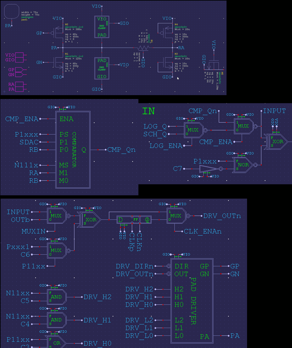
Dunno. But the feedback can be unregistered within the pad-ring, therefore completely unhindered by clocking. PA is electrical pin -> 600 ohm resistor to RA -> comparator -> CMP_Qn -> INPUT -> optional inverter/flip-flop -> DRV_OUTn -> pad driver -> PA.
Thanks evanh, for providing the information/schematics!
It seems fantastic, because then we can completelly dismiss the someway low-valued pull-ups (in the "purist" sense of comparator feedback) and make use of the 1uA or 10uA-drive modes, which would simulate the insertion of one 3M3 Ohm or 330 kOmh resistor, respectivelly.
As seen by the comparator, the 600 Ohm series-resistor is after PA node, thus it can be thought as an input protection, limiting the amount of current/energy that reaches the analog amplifier, but it also lowers the rate of charge/discharge of any capacitances in amplifier's input-path.
With PA as the summing node, the control loop will be capable of selecting the drive-level (0, 1 or 10 uA) which better suits each situation, since the intent is to emulate the steepy-response of an open drain output that abbruptly changes its polarity, totally compatible whith fast settling-time comparators.
I foresee some really good times ahead, for analog designers using P2.
Every comparator has a hysteresis. Otherwise the circuit would oscillate due to its own noise.
I totally agree, but the "normal" level of internally-provided hysteresis uses to be very low in some of the fast comparators whose datasheets I've been studying, in the order of 6 mV, a level value wich can be found as insufficient to fit every possible situation, including, but not limited, to any "contamination", due any power supply noise level.
That's the reason I've been thinking about using any eventual current-feedback, and open-drain-output emmulation possibilities, as some useful means for improveing the chances for internal comparator's useability.
Here's a link to a very informative document, from Texas Instruments-training site (as provided by Google search):
https://training.ti.com/sites/default/files/effective-application-of-analog-comparators.pdf
During the last part of today's meeting I've asked Chip if the comparators embodied at the pins do have any hysteresis, even a minimum, by design.
The answer was no, there's not any preset value for the hysteresis, because there is no intentional feedback path designed into it.
I understand it as some good news, because it opens a lot of opportunities for clever designs, able to "explore" that reality.
By making use of the many resources available at the pins themselves, one will be able to configure their input/output terminations and driving capabilities, modifying the control bits responsible for the final routing of their connection paths towards Vio and Gio, thus affecting the voltages present at the input nodes.
Another possibility would be resorting to majority-voting, in order to calculate the final result of any comparisons, but this is a time-consuming technic, only useful in the less critical designs.
In some cases, the raw reading of the comparator could be enough, e.g., when comparing a square wave signal with a sine wave one.
Lots of possibilities open for experimentation.
Good times ahead!
Ok, no negative feedback / switching hysteresis.
I suspect a RC compensation to suppress the natural oscillation tendency at the switching point of both input voltages.
What is the smallest voltage difference that does not lead to misinterpretations (e.g. inherent noise)?
With the DAC there is the problem that it does not work from 0...3.3V.
In which voltage range does the comparator work?
The DACs are rail-to-rail, 0 .. 3.3 V.
I suspect you mean the ADCs having a numerical span of 5 Volts. It's in the nature of sigma-delta that there is no defined rails. Chip chose to expand the span beyond the rails rather than approximating them then having error that misses the mark.
So the real issue is not what the ADC span is but that there is DC drift.
If the error is known everything is no problem.
It's not known because it drifts over time. That's why I'd said the published ENOB table is something like >10 Hz bandpass.