Yeah I know, maybe enough for PAL/NTSC res @ 8bpp or something...be quite good if I got 16bpp or more to prove it is actually reading from external RAM.
LOL. It works with real SRAM! Well at 4MHz right now, anyway.
Enter command (?=HELP) : G
Enter destination for random data [R]am, [S]cratch : S
Enter offset address to write to [0] : 0
Enter number of random bytes to write (hex) [0] : 100

Generating random data

Enter command (?=HELP) : D
Enter source, [R]AM, [H]ub, [S]cratch : S
Enter size, [B]ytes, [W]ords, [L]ongs : B
Enter offset address to dump [0] : 0
SCRATCH 00000000 (00000000)  : DD 60 AA 3D 9C 10 B1 69 C1 8D 99 C0 2D FC 6A 39  .`.=...i....-.j9
SCRATCH 00000010 (00000010)  : 57 5F F6 30 F3 31 03 64 3E B6 35 2A 98 6D 2B 83  W_.0.1.d>.5*.m+.
SCRATCH 00000020 (00000020)  : 01 26 09 45 DA 73 A6 54 8E 47 03 7F 9D 91 3A 76  .&.E.s.T.G...:v
SCRATCH 00000030 (00000030)  : F3 FC 02 F4 B8 F9 E1 CA 47 50 98 5C DA 32 EC 58  ........GP.\.2.X
SCRATCH 00000040 (00000040)  : C7 3C 23 75 88 67 52 68 39 22 65 99 29 6D C9 A4  .<#u.gRh9"e.)m..
SCRATCH 00000050 (00000050)  : F3 BD 6C 03 D6 42 59 F5 2E 40 26 C4 F2 D1 75 C6  ..l..BY..@&...u.
SCRATCH 00000060 (00000060)  : F4 C4 02 31 82 90 F8 64 47 CE 8C D5 46 4D BF 07  ...1...dG...FM..
SCRATCH 00000070 (00000070)  : 03 BA 98 62 F6 D1 C1 59 D8 84 C4 66 0D 80 B5 F5  ...b...Y...f....
SCRATCH 00000080 (00000080)  : 8D 5E 60 37 20 E1 C7 13 49 8F 81 F7 14 A6 08 E0  .^`7 ...I.......
SCRATCH 00000090 (00000090)  : 01 0E 01 51 F1 57 60 4A DC 01 F1 0A C3 9B AA A8  ...Q.W`J........
SCRATCH 000000A0 (000000A0)  : D6 D2 5A B2 F1 65 12 1E B6 F8 F2 05 EF 36 03 4B  ..Z..e.......6.K
SCRATCH 000000B0 (000000B0)  : 1C DB 80 11 F0 4E C9 E3 05 46 F0 18 A2 E3 AF 50  .....N...F.....P
SCRATCH 000000C0 (000000C0)  : 17 93 23 A0 E1 D7 08 DF 3F 64 26 E4 3B 76 CE 11  ..#.....?d&.;v..
SCRATCH 000000D0 (000000D0)  : 0F 6E F8 C1 93 3F B2 CB DE EF BB 6B 4B 57 F8 7C  .n...?.....kKW.|
SCRATCH 000000E0 (000000E0)  : 41 1A DC 05 E6 8A A1 AE 5B CF D8 4A 7D E1 BD DD  A.......[..J}...
SCRATCH 000000F0 (000000F0)  : 91 8A 4B 64 96 E4 1A 74 F7 4C 36 11 E9 6A 9A CE  ..Kd...t.L6..j..

Enter command (?=HELP) : M
Enter source, [R]AM, [H]ub, [S]cratch : S
Enter destination, [R]AM, [S]cratch : R
Enter source offset address [0] : 0
Enter destination offset address [0] : 0
Enter number of bytes to copy (hex) [1]: 100
Transferred 256 bytes

Enter command (?=HELP) : D
Enter source, [R]AM, [H]ub, [S]cratch : R
Enter size, [B]ytes, [W]ords, [L]ongs : B
Enter offset address to dump [0] : 0
PSRAM 00000000 (00000000) : DD 60 AA 3D 9C 10 B1 69 C1 8D 99 C0 2D FC 6A 39  .`.=...i....-.j9
PSRAM 00000010 (00000010) : 57 5F F6 30 F3 31 03 64 3E B6 35 2A 98 6D 2B 83  W_.0.1.d>.5*.m+.
PSRAM 00000020 (00000020) : 01 26 09 45 DA 73 A6 54 8E 47 03 7F 9D 91 3A 76  .&.E.s.T.G...:v
PSRAM 00000030 (00000030) : F3 FC 02 F4 B8 F9 E1 CA 47 50 98 5C DA 32 EC 58  ........GP.\.2.X
PSRAM 00000040 (00000040) : C7 3C 23 75 88 67 52 68 39 22 65 99 29 6D C9 A4  .<#u.gRh9"e.)m..
PSRAM 00000050 (00000050) : F3 BD 6C 03 D6 42 59 F5 2E 40 26 C4 F2 D1 75 C6  ..l..BY..@&...u.
PSRAM 00000060 (00000060) : F4 C4 02 31 82 90 F8 64 47 CE 8C D5 46 4D BF 07  ...1...dG...FM..
PSRAM 00000070 (00000070) : 03 BA 98 62 F6 D1 C1 59 D8 84 C4 66 0D 80 B5 F5  ...b...Y...f....
PSRAM 00000080 (00000080) : 8D 5E 60 37 20 E1 C7 13 49 8F 81 F7 14 A6 08 E0  .^`7 ...I.......
PSRAM 00000090 (00000090) : 01 0E 01 51 F1 57 60 4A DC 01 F1 0A C3 9B AA A8  ...Q.W`J........
PSRAM 000000A0 (000000A0) : D6 D2 5A B2 F1 65 12 1E B6 F8 F2 05 EF 36 03 4B  ..Z..e.......6.K
PSRAM 000000B0 (000000B0) : 1C DB 80 11 F0 4E C9 E3 05 46 F0 18 A2 E3 AF 50  .....N...F.....P
PSRAM 000000C0 (000000C0) : 17 93 23 A0 E1 D7 08 DF 3F 64 26 E4 3B 76 CE 11  ..#.....?d&.;v..
PSRAM 000000D0 (000000D0) : 0F 6E F8 C1 93 3F B2 CB DE EF BB 6B 4B 57 F8 7C  .n...?.....kKW.|
PSRAM 000000E0 (000000E0) : 41 1A DC 05 E6 8A A1 AE 5B CF D8 4A 7D E1 BD DD  A.......[..J}...
PSRAM 000000F0 (000000F0) : 91 8A 4B 64 96 E4 1A 74 F7 4C 36 11 E9 6A 9A CE  ..Kd...t.L6..j..

Enter command (?=HELP) : C
Enter source 1 to compare, [R]AM, [H]ub, [S]cratch : R
Enter source 2 to compare, [R]AM, [H]ub, [S]cratch : S
Enter source 1 offset address to read from [0] : 0
Enter source 2 offset address to read from [0] : 0
Enter number of bytes to compare (hex) [0]: 100

Comparing memory.
Memory range matches

Enter command (?=HELP) :
Here's me linear block read using a streamer at sysclock/2. Of note is no smartpin since it was only doing WE pulsing for writes.
The use of XINIT + XCONT works really well (hopefully, since I've not tested it) for I/O latency compensation. A WAITX wouldn't work anyway, at sysclock/2, since address generation is already 100% consuming the cog prior to read data arriving.
con
    CEPIN       = 8
    OEPIN       = CEPIN+1
    WEPIN       = CEPIN+2
    DATABUS_GRP = 0<<20

dat

sram_rdblock
        wrfast  fifo_nb, hub_addr   'prep the FIFO
        mov outa, sr_addr       'preset address bus, includes CE  (This will clobber any preceding OUTA actions!)
        andn    dira, #$ff      'tristate the 8-bit data bus
        or  outa, srcmd_rd      'start the read operation

        xinit   stm_immrd, #0       'preamble the streamer for I/O latency, takes two ticks to start
        setword stm_wf8, length, #0 'count of streamer transfer cycles
        xcont   stm_wf8, #0     'SRAM data read -> streamer -> FIFO -> hubRAM

        rep @.rloop, length     'cycle through the addresses
        add outa, srcmd_add     'sr_addr + 1 -> SRAM address bus
.rloop
        andn    outa, srcmd_not     'release SRAM
        or  dira, #$ff      'drive the 8-bit data bus

        waitxfi             'wait until final byte arived from SRAM -> streamer -> FIFO
    _ret_   rdfast  fifo_nb, #0     'empty remaining FIFO data -> hubRAM


stm_immrd   long    X_IMM_4X8_1DAC8 | DATABUS_GRP | 8       ' 16 sysclock ticks
stm_rf8     long    X_RFBYTE_8P_1DAC8 | X_PINS_ON | DATABUS_GRP
stm_wf8     long    X_8P_1DAC8_WFBYTE | X_PINS_ON | DATABUS_GRP
fifo_nb     long    $8000_0000      'FIFO non-blocking mode

srcmd_ce    long    %0001<<CEPIN        'CE only
srcmd_rd    long    %0011<<CEPIN        'OE and CE
srcmd_wr    long    %0101<<CEPIN        'WE and CE
srcmd_wrn   long    %0100<<CEPIN        'invert WE
srcmd_not   long    %0111<<CEPIN        'release SRAM
srcmd_add   long    %1000<<CEPIN        'sr_addr + 1
@rogloh said:
LOL. It works with real SRAM! Well at 4MHz right now, anyway.
Nice. And 4 MHz is a good choice for that wiring.
Yeah I will try higher and see where things top out. If I find I can get at least SD video out of it I'll be somewhat pleased.
Otherwise to go further requires laying out a PCB etc and using some fast RAM.
Update: appears to be working at a P2 clock of 40MHz (interactively at least). This would be a 50ns cycle at sysclk/2. I think this memory is not quite rated that fast. Once I hookup video it'll be obvious when errors happen.
I've commented my post above now. I'm pretty chuffed with it. Party because I've really got a feel for the streamer now. I've not tested that code above but I'm pretty sure I've correctly used the streamer. It's a nice trick for preambling if it works as expected.
Yeah just checked your code, you've pretty much used the same approach I did in the end. XINIT to pad, XCONT and REP with address increment. Works a treat. I have the address bus starting at 0 or 32, control pins can be put anywhere, and data bus can be on some 8 bit boundary (including the second port). It makes sense to put CS one higher than the top address bit or leave empty so any rollover of 4 or 2 byte quantities read at the top of memory after incrementing the address will only drive CS high (I don't invert CS/OE signals, just the WE). Alternatively you could put WE here as it is not driven by OUTA state, just the smartpin logic.
Oh man, this is low frequency operation and my video is not working perfectly with this SRAM yet. I am running the P2 at 40.5MHz and the NTSC dotclock at 13.5MHz. I'm thinking I'm plagued by noise with that breadboard as I see random pixels errors. But I do see a picture of sorts at times. It's nasty. I'll need to see if things can be improved tomorrow or if I'm stuck until some PCB is made for higher speed SRAM testing.
Static placement of bad pixels. I've been hunting this down for a few hours. It happens even at 4MHz P2 operation. It's quite weird. If I write to a RAM address and read it back it looks like the data takes okay, but if I wait a while and read it back later it can read some bit errors. If I fix the error by writing back to this address the data I wanted, from then on it seems okay and will read correctly and repeatedly after this. The strange thing is writing to the SRAM memory seems to take the first time, then appear to "decay" a bit later. Errors don't seem to be at the same address but it is a commonly bit 1 or 2 being affected.
It could well be because I am using 5V CMOS RAM at 3.3V too, that's all I have in DIP unfortunately. I've probed the output signal and it seems to drive out okay and in time (rising transition is a little slow, but at 4-20MHz it's mostly fine). Maybe the input logic levels are bad and there is some metastability or something else weird going on.
Update:
Looking at the video output, bad pixels are always at fixed positions. It's like some addresses in the SRAM are just bad. They also do automatically self corrupt again if I continue to write to them (see code below). These bad pixels reappear within one second of being re-written with the correct data. I tried to align the screen with a power of 2 as well to see if that showed me anything but didn't see any obvious patterns, although many bad columns do have more that one bad pixel in them.
    repeat j from 0 to 100
        repeat i from 0 to 511
            mem.writeByte(HYPRAM_ADDR+i+(j<<9), byte[@pic+$436][i+(j*720)])
    repeat
        repeat j from 0 to 100
            repeat i from 0 to 511
                if mem.readByte(HYPRAM_ADDR+i+(j<<9)) <> byte[@pic+$436][i+(j*720)]
                    mem.writeByte(HYPRAM_ADDR+i+(j<<9), byte[@pic+$436][i+j*720])
        waitms(1000)
I think it's probably some bad connections. If I wiggle the address bus cables the bad pixels all move to different locations and increase in number. So perhaps some address signals are not getting through reliably. It's a pretty crappy setup.
@rogloh said:
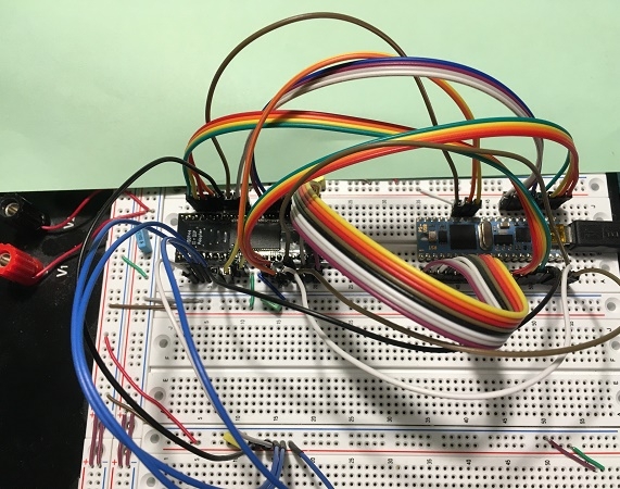
Just wired up this abomination with that DIP SRAM I had laying about!
Very inspiring - i have now wired up my sram to test if the dip adapter actually works, looks similar
Using a P1 to test it as my P2 board is in use at the moment.
After some wiggling with the cables memory read write tests give no errors
I hope I can get a P2 setup going soon and test all the great suggestions posted here!
@aaaaaaaargh In general unless you already have the memories and enough P2 pins free, SRAM is probably going to be a more costly way to get video memory on the P2 vs PSRAM, if those PSRAM chips are now under a dollar each. SRAM is far simpler to control in principle though so I can see the attraction using it vs the PSRAM and HyperRAM approaches and it may offer lower latencies when directly coupled to a COG, so probably better for emulators etc. You can transfer far longer bursts unimpeded by any refresh requirements too. You only need to deal with the possible address wraparounds during the burst transfers so the address bus change doesn't affect other output pins on the same port. You could get around that restriction by keeping the data bus and control pins on the other port to the address bus.
To save pins, increase density and improve video bandwidth, you might want to consider using PSRAM in SOIC-8 as that's very easy to solder yourself. It's just somewhat more complex to code and has higher latency. You will find that breadboard memory performance is going to be low and you'll start to get signal integrity issues as the frequency increases. Of course it's fine just to get things started though.
One reasonable compromise to reduce SRAM pin usage from 32 (for a 2MB SRAM) down to just 20 or 19 pins would be to use a multiplexed bus setup with a pair of 8 bit latches (or a single 16 bit one) attached as follows:
P0-P7 is wired to D0-D7 and also to the inputs to 8 bit latch 1 which is feeding its outputs to A8-A15 of SRAM
P8-P15 is wired directly to A0-A7 and also to the inputs of 8 bit latch 2 which is feeding its outputs to A16-A23 of SRAM
P16 - CS (or CS+ALE combined)
P17 - WR
P18 - RD
P19 - ALE (transparent)
The P2 could then write A8-A23 (so it supports up to 16MB) on P0-P15 and transparently latch with ALE falling edge (ALE might be sharable with CS that way)
The P2 would then output A7-A0 on P8-P15 and increment the output port by 256 within a burst, which increases adresses A7-A0.
This would allow bursts of up to 256 bytes in a "page" before the latches need to be re-written, ensuring a decent burst transfer rate. It could also be extended to have more SRAM banks on the same port (with an additional CS pin for each).
Probably CS can be combined with ALE and 19 pins is then only a one more pin than 18 for 4xPSRAMs in the 16 bit arrangement. It saves at least one chip (2 or 3 chips vs 4) but the downside is the board wiring is more complete to route and it transfers 8 bits at sysclk/2 instead of 16 at sysclk/2 for the PSRAM. Pin count is more reasonable though. You could pack the 16 bit transparent latch into a single CPLD with only 25 I/O pins needed on the CPLD or just use a 74ALVT16373T.
Update: Also there may be some scope to use 16 bit wide SRAM too with a different latch arrangement and more P2 pins used. This could potentially then yield the same bandwidth as 16 bit wide PSRAM. ISSI make some high speed 16 bit SRAMs which could be of interest.
@rogloh said:
(ALE might be sharable with CS that way)
I would not recommend doing that. The SRAM chips I've spent my time with have poor specifications for enabling /CS. For example, the Cypress chip I have in mind has signals /OE and /CE, for output enable and chip enable, respectively - The data valid times from /CE are nearly double those from /OE. For the -15 spec chip, data valid from OE is max 7ns, while from CE it's 15ns. S.
ETA: Other SRAMs look similar. A Samsung -70 [ns] chip specifies a max time of 35ns from /OE, but 70ns from /CE.
It's okay if you have other code to run in the meantime, like enabling buses, or setting up clocks for writes etc where this lag can be utilized. But it would be good to have the option of both types.
I wrote before about using small CPLD/FPGA (like ICE40 or 10M02), and have not been the only one to think about that. Today I was looking for some Si5351 modules (mentioned by rogloh in another thread) and ended up finding small FPGA (actually tinyFPGA AX).
Two or three more google shearches later I found his website. And four-five google searches later I found that he's even registered in the forums ('TinyFPGA' but not active since 2018).
Will a message @TinyFPGA send him some email? Maybe he can provide his opinion about mixing Lattice XO2/ICE40 with some PSRAM/SRAM/SDRAM/HyperRAM. The idea is having something that just 'glues' well with P2. rogloh knows what is needed on SW side, TinyFPGA could maybe help to put ideas into practice.
@Ramon said:
Will a message @TinyFPGA send him some email? Maybe he can provide his opinion about mixing Lattice XO2/ICE40 with some PSRAM/SRAM/SDRAM/HyperRAM. The idea is having something that just 'glues' well with P2. rogloh knows what is needed on SW side, TinyFPGA could maybe help to put ideas into practice.
I would say that a P2 in general shouldn't tend to need any glue between these devices - HyperRAM and PSRAM are easily directly accessed. For SRAM, a CPLD or other latch logic can be useful for reducing pin counts in a multiplexed arrangement vs being directly attached, but direct attachment still works out fine, at least for video RAM application where bandwidth is more important than latency. I think it's much easier to get things working sooner when controlled by the P2 vs building in additional FPGA/CPLD logic. Admittedly SDRAM will be more complex to control but I'm thinking if self-refresh can be used for ALL refreshing and the burst size is enforced like is already being done with the PSRAM and HyperRAM, then this should be doable as well. Unless you are after the smallest latency possible or cannot tolerate interrupted burst transfers, it's worth looking into using PSRAM or HyperRAM to see if that is suitable for the application. But I'd hope to support all of these RAM types in my memory driver in the end if possible.
@rogloh said:
One reasonable compromise to reduce SRAM pin usage from 32 (for a 2MB SRAM) down to just 20 or 19 pins would be to use a multiplexed bus setup with a pair of 8 bit latches (or a single 16 bit one) attached as follows:
P0-P7 is wired to D0-D7 and also to the inputs to 8 bit latch 1 which is feeding its outputs to A8-A15 of SRAM
P8-P15 is wired directly to A0-A7 and also to the inputs of 8 bit latch 2 which is feeding its outputs to A16-A23 of SRAM
P16 - CS (or CS+ALE combined)
P17 - WR
P18 - RD
P19 - ALE (transparent)
The P2 could then write A8-A23 (so it supports up to 16MB) on P0-P15 and transparently latch with ALE falling edge (ALE might be sharable with CS that way)
The P2 would then output A7-A0 on P8-P15 and increment the output port by 256 within a burst, which increases adresses A7-A0.
This would allow bursts of up to 256 bytes in a "page" before the latches need to be re-written, ensuring a decent burst transfer rate. It could also be extended to have more SRAM banks on the same port (with an additional CS pin for each).
Probably CS can be combined with ALE and 19 pins is then only a one more pin than 18 for 4xPSRAMs in the 16 bit arrangement. It saves at least one chip (2 or 3 chips vs 4) but the downside is the board wiring is more complete to route and it transfers 8 bits at sysclk/2 instead of 16 at sysclk/2 for the PSRAM. Pin count is more reasonable though. You could pack the 16 bit transparent latch into a single CPLD with only 25 I/O pins needed on the CPLD or just use a 74ALVT16373T.
Update: Also there may be some scope to use 16 bit wide SRAM too with a different latch arrangement and more P2 pins used. This could potentially then yield the same bandwidth as 16 bit wide PSRAM. ISSI make some high speed 16 bit SRAMs which could be of interest.
Presettable 8-bit counter (requires external gate for cascading)
then you can also extend bursts length as the addresses can self-increment.
By widening the data bus to 16b of course you will also widen the address preset
@rogloh said: those PSRAM chips are now under a dollar each..... you might want to consider using PSRAM in SOIC-8 as that's very easy to solder yourself.
Do you have an example of such a psram?
I have tested SOIC-8 PSRAM in the past, namely the ESP-PSRAM64H. Thats a 64Mbit psram (8Mx8) with SPI and QPI. The problem with that one was that there was no way to tell if it needed some time to refresh. So writing bursts in linear mode (>256kb) resulted in invalid data. I found this with 3 differrent Chips and thus abandoned any further attempts using psram - but if I understand it correctly then other psram chips have a mechanism to signal if they need a timeout.
Presettable 8-bit counter (requires external gate for cascading)
then you can also extend bursts length as the addresses can self-increment.
By widening the data bus to 16b of course you will also widen the address preset
Yeah you could do that, and it would just take one more P2 control pin to increment the counter. As it is only occurring once in every 256 transfers during a long burst, any gain of pulsing this clock pin (2 instructions) vs relatching (maybe ~7-8 instructions?) is scaled down so it might only increase performance marginally, e.g. ~1% boost?
@rogloh said: those PSRAM chips are now under a dollar each..... you might want to consider using PSRAM in SOIC-8 as that's very easy to solder yourself.
Do you have an example of such a psram?
I have tested SOIC-8 PSRAM in the past, namely the ESP-PSRAM64H. Thats a 64Mbit psram (8Mx8) with SPI and QPI. The problem with that one was that there was no way to tell if it needed some time to refresh. So writing bursts in linear mode (>256kb) resulted in invalid data. I found this with 3 differrent Chips and thus abandoned any further attempts using psram - but if I understand it correctly then other psram chips have a mechanism to signal if they need a timeout.
Yeah that ESP PSRAM is the exact sort of device I am talking about and is what my driver supports. It needs time to self-refresh so you have to fragment your bursts to leave it time to refresh. Don't exceed 8us or cross the page boundary at full speed and things are ok. For video use it is not much of an issue.
Incidentally, I was poking around Digikey's website, and they had two 4Mx8 chips available for rather a lot less money than one 8Mx8 ($15ish vs. $10ish, USD) - and more options, too. S.
@rogloh said: that ESP PSRAM is the exact sort of device I am talking about and is what my driver supports.
Eeeeh @rogloh , I have been looking at that driver, I'm assuming you mean p2videodrv.spin. V0.93 is the newest I can find - but it says 0.92b 15 FEB 2021 in the doc file.
I can't find any reference or info in there on how to use PSRAM m I looking at the correct driver? I wanted to see if this could be modified to use sram.
Ok that's my video driver and the newest one can request frame buffer data from external RAM, but I was mainly talking about my memory driver which is required to read the memory devices. Yes the video documentation is getting out of date and probably does not cover the latest external memory support available as things have changed slightly in that area.
Only my HyperRAM/HyperFlash memory driver has been released so far. I've not yet released the PSRAM one because boards using PSRAM are not widely available from Parallax yet, but that memory driver is all feature complete and well tested with no known bugs left. I also now have an experimental SRAM version coded up as well that I hacked up in a couple of days last week. It is not yet well tested because all I have for testing it is that breadboard setup above which had problems, but it still appears to function at the lower speeds I ran. I could only release it as an alpha if I were do so now, it's a bit too raw and unoptimized and still slightly hard coded in its setup. The main thing left I still need to do is to get these new variants properly integrated into my higher level SPIN2 memory driver "wrapper" layer (memory.spin2). As it is coded today this wrapper layer is primarily designed to support Hyper memory which is where the whole project started from, but it now needs to change slightly to become more generic and accommodate all these different RAM types so some setup APIs and common constants etc still need to be moved around or tweaked. I have to figure out how to do that cleanly, perhaps using some method pointers in SPIN2. The idea is that any memory driver can be just dropped in to provide external memory access to COGs so they won't need to change much, just the device initialization differs and that is what I need to work on.
Are you just after some SRAM access routines for your own driver to use or do you want a full SRAM driver compatible with my video driver? There's no need to start from PSRAM/HyperRAM and try to create another SRAM one, as I've already taken that step, or at least 98% of it. I'm just trying to make it easier to use which I find is one of the harder parts to this.
Also as I discovered, without a proper PCB it is likely you'll find that your breadboard will not be able to run particularly fast. Hopefully you could get some VGA output if the signal integrity allows it to reach into the 25-50MHz range.
Are you just after some SRAM access routines for your own driver to use or do you want a full SRAM driver compatible with my video driver? There's no need to start from PSRAM/HyperRAM and try to create another SRAM one, as I've already taken that step, or at least 98% of it. I'm just trying to make it easier to use which I find is one of the harder parts to this.
Ideally I would like to use your video driver. It’s so flexible and if it could support different kinds of external memory that could be used for storage as well as vga - that would be the ideal.


Comments
Yeah I know, maybe enough for PAL/NTSC res @ 8bpp or something...be quite good if I got 16bpp or more to prove it is actually reading from external RAM.
LOL. It works with real SRAM! Well at 4MHz right now, anyway.
Here's me linear block read using a streamer at sysclock/2. Of note is no smartpin since it was only doing WE pulsing for writes.
The use of XINIT + XCONT works really well (hopefully, since I've not tested it) for I/O latency compensation. A WAITX wouldn't work anyway, at sysclock/2, since address generation is already 100% consuming the cog prior to read data arriving.
con CEPIN = 8 OEPIN = CEPIN+1 WEPIN = CEPIN+2 DATABUS_GRP = 0<<20 dat sram_rdblock wrfast fifo_nb, hub_addr 'prep the FIFO mov outa, sr_addr 'preset address bus, includes CE (This will clobber any preceding OUTA actions!) andn dira, #$ff 'tristate the 8-bit data bus or outa, srcmd_rd 'start the read operation xinit stm_immrd, #0 'preamble the streamer for I/O latency, takes two ticks to start setword stm_wf8, length, #0 'count of streamer transfer cycles xcont stm_wf8, #0 'SRAM data read -> streamer -> FIFO -> hubRAM rep @.rloop, length 'cycle through the addresses add outa, srcmd_add 'sr_addr + 1 -> SRAM address bus .rloop andn outa, srcmd_not 'release SRAM or dira, #$ff 'drive the 8-bit data bus waitxfi 'wait until final byte arived from SRAM -> streamer -> FIFO _ret_ rdfast fifo_nb, #0 'empty remaining FIFO data -> hubRAM stm_immrd long X_IMM_4X8_1DAC8 | DATABUS_GRP | 8 ' 16 sysclock ticks stm_rf8 long X_RFBYTE_8P_1DAC8 | X_PINS_ON | DATABUS_GRP stm_wf8 long X_8P_1DAC8_WFBYTE | X_PINS_ON | DATABUS_GRP fifo_nb long $8000_0000 'FIFO non-blocking mode srcmd_ce long %0001<<CEPIN 'CE only srcmd_rd long %0011<<CEPIN 'OE and CE srcmd_wr long %0101<<CEPIN 'WE and CE srcmd_wrn long %0100<<CEPIN 'invert WE srcmd_not long %0111<<CEPIN 'release SRAM srcmd_add long %1000<<CEPIN 'sr_addr + 1Nice. And 4 MHz is a good choice for that wiring.
Yeah I will try higher and see where things top out. If I find I can get at least SD video out of it I'll be somewhat pleased.
Otherwise to go further requires laying out a PCB etc and using some fast RAM.
Update: appears to be working at a P2 clock of 40MHz (interactively at least). This would be a 50ns cycle at sysclk/2. I think this memory is not quite rated that fast. Once I hookup video it'll be obvious when errors happen.
Are you using the streamer for reading the SRAM?
Yes but no smart pin. It needs some streamer command tweaking to get the delay right to line up with when the address changes. Works fine for bursts.
I've commented my post above now. I'm pretty chuffed with it. Party because I've really got a feel for the streamer now. I've not tested that code above but I'm pretty sure I've correctly used the streamer. It's a nice trick for preambling if it works as expected.
Yeah just checked your code, you've pretty much used the same approach I did in the end. XINIT to pad, XCONT and REP with address increment. Works a treat. I have the address bus starting at 0 or 32, control pins can be put anywhere, and data bus can be on some 8 bit boundary (including the second port). It makes sense to put CS one higher than the top address bit or leave empty so any rollover of 4 or 2 byte quantities read at the top of memory after incrementing the address will only drive CS high (I don't invert CS/OE signals, just the WE). Alternatively you could put WE here as it is not driven by OUTA state, just the smartpin logic.
Cool. I didn't know you had that one in your kit.
Oh man, this is low frequency operation and my video is not working perfectly with this SRAM yet. I am running the P2 at 40.5MHz and the NTSC dotclock at 13.5MHz. I'm thinking I'm plagued by noise with that breadboard as I see random pixels errors. But I do see a picture of sorts at times. It's nasty. I'll need to see if things can be improved tomorrow or if I'm stuck until some PCB is made for higher speed SRAM testing.
Are the speckles a random shimmer or static placement? Or a bit of both?
Static placement of bad pixels. I've been hunting this down for a few hours. It happens even at 4MHz P2 operation. It's quite weird. If I write to a RAM address and read it back it looks like the data takes okay, but if I wait a while and read it back later it can read some bit errors. If I fix the error by writing back to this address the data I wanted, from then on it seems okay and will read correctly and repeatedly after this. The strange thing is writing to the SRAM memory seems to take the first time, then appear to "decay" a bit later. Errors don't seem to be at the same address but it is a commonly bit 1 or 2 being affected.
It could well be because I am using 5V CMOS RAM at 3.3V too, that's all I have in DIP unfortunately. I've probed the output signal and it seems to drive out okay and in time (rising transition is a little slow, but at 4-20MHz it's mostly fine). Maybe the input logic levels are bad and there is some metastability or something else weird going on.
Update:
Looking at the video output, bad pixels are always at fixed positions. It's like some addresses in the SRAM are just bad. They also do automatically self corrupt again if I continue to write to them (see code below). These bad pixels reappear within one second of being re-written with the correct data. I tried to align the screen with a power of 2 as well to see if that showed me anything but didn't see any obvious patterns, although many bad columns do have more that one bad pixel in them.
repeat j from 0 to 100 repeat i from 0 to 511 mem.writeByte(HYPRAM_ADDR+i+(j<<9), byte[@pic+$436][i+(j*720)]) repeat repeat j from 0 to 100 repeat i from 0 to 511 if mem.readByte(HYPRAM_ADDR+i+(j<<9)) <> byte[@pic+$436][i+(j*720)] mem.writeByte(HYPRAM_ADDR+i+(j<<9), byte[@pic+$436][i+j*720]) waitms(1000)I think it's probably some bad connections. If I wiggle the address bus cables the bad pixels all move to different locations and increase in number. So perhaps some address signals are not getting through reliably. It's a pretty crappy setup.
's beautiful.")
S.
Very inspiring - i have now wired up my sram to test if the dip adapter actually works, looks similar
Using a P1 to test it as my P2 board is in use at the moment.
After some wiggling with the cables memory read write tests give no errors
I hope I can get a P2 setup going soon and test all the great suggestions posted here!
@aaaaaaaargh In general unless you already have the memories and enough P2 pins free, SRAM is probably going to be a more costly way to get video memory on the P2 vs PSRAM, if those PSRAM chips are now under a dollar each. SRAM is far simpler to control in principle though so I can see the attraction using it vs the PSRAM and HyperRAM approaches and it may offer lower latencies when directly coupled to a COG, so probably better for emulators etc. You can transfer far longer bursts unimpeded by any refresh requirements too. You only need to deal with the possible address wraparounds during the burst transfers so the address bus change doesn't affect other output pins on the same port. You could get around that restriction by keeping the data bus and control pins on the other port to the address bus.
To save pins, increase density and improve video bandwidth, you might want to consider using PSRAM in SOIC-8 as that's very easy to solder yourself. It's just somewhat more complex to code and has higher latency. You will find that breadboard memory performance is going to be low and you'll start to get signal integrity issues as the frequency increases. Of course it's fine just to get things started though.
One reasonable compromise to reduce SRAM pin usage from 32 (for a 2MB SRAM) down to just 20 or 19 pins would be to use a multiplexed bus setup with a pair of 8 bit latches (or a single 16 bit one) attached as follows:
P0-P7 is wired to D0-D7 and also to the inputs to 8 bit latch 1 which is feeding its outputs to A8-A15 of SRAM
P8-P15 is wired directly to A0-A7 and also to the inputs of 8 bit latch 2 which is feeding its outputs to A16-A23 of SRAM
P16 - CS (or CS+ALE combined)
P17 - WR
P18 - RD
P19 - ALE (transparent)
The P2 could then write A8-A23 (so it supports up to 16MB) on P0-P15 and transparently latch with ALE falling edge (ALE might be sharable with CS that way)
The P2 would then output A7-A0 on P8-P15 and increment the output port by 256 within a burst, which increases adresses A7-A0.
This would allow bursts of up to 256 bytes in a "page" before the latches need to be re-written, ensuring a decent burst transfer rate. It could also be extended to have more SRAM banks on the same port (with an additional CS pin for each).
Probably CS can be combined with ALE and 19 pins is then only a one more pin than 18 for 4xPSRAMs in the 16 bit arrangement. It saves at least one chip (2 or 3 chips vs 4) but the downside is the board wiring is more complete to route and it transfers 8 bits at sysclk/2 instead of 16 at sysclk/2 for the PSRAM. Pin count is more reasonable though. You could pack the 16 bit transparent latch into a single CPLD with only 25 I/O pins needed on the CPLD or just use a 74ALVT16373T.
Update: Also there may be some scope to use 16 bit wide SRAM too with a different latch arrangement and more P2 pins used. This could potentially then yield the same bandwidth as 16 bit wide PSRAM. ISSI make some high speed 16 bit SRAMs which could be of interest.
I would not recommend doing that. The SRAM chips I've spent my time with have poor specifications for enabling /CS. For example, the Cypress chip I have in mind has signals /OE and /CE, for output enable and chip enable, respectively - The data valid times from /CE are nearly double those from /OE. For the -15 spec chip, data valid from OE is max 7ns, while from CE it's 15ns. S.
ETA: Other SRAMs look similar. A Samsung -70 [ns] chip specifies a max time of 35ns from /OE, but 70ns from /CE.
It's okay if you have other code to run in the meantime, like enabling buses, or setting up clocks for writes etc where this lag can be utilized. But it would be good to have the option of both types.
I wrote before about using small CPLD/FPGA (like ICE40 or 10M02), and have not been the only one to think about that. Today I was looking for some Si5351 modules (mentioned by rogloh in another thread) and ended up finding small FPGA (actually tinyFPGA AX).
Two or three more google shearches later I found his website. And four-five google searches later I found that he's even registered in the forums ('TinyFPGA' but not active since 2018).
Will a message @TinyFPGA send him some email? Maybe he can provide his opinion about mixing Lattice XO2/ICE40 with some PSRAM/SRAM/SDRAM/HyperRAM. The idea is having something that just 'glues' well with P2. rogloh knows what is needed on SW side, TinyFPGA could maybe help to put ideas into practice.
I would say that a P2 in general shouldn't tend to need any glue between these devices - HyperRAM and PSRAM are easily directly accessed. For SRAM, a CPLD or other latch logic can be useful for reducing pin counts in a multiplexed arrangement vs being directly attached, but direct attachment still works out fine, at least for video RAM application where bandwidth is more important than latency. I think it's much easier to get things working sooner when controlled by the P2 vs building in additional FPGA/CPLD logic. Admittedly SDRAM will be more complex to control but I'm thinking if self-refresh can be used for ALL refreshing and the burst size is enforced like is already being done with the PSRAM and HyperRAM, then this should be doable as well. Unless you are after the smallest latency possible or cannot tolerate interrupted burst transfers, it's worth looking into using PSRAM or HyperRAM to see if that is suitable for the application. But I'd hope to support all of these RAM types in my memory driver in the end if possible.
If you replace the external latch eg with this
then you can also extend bursts length as the addresses can self-increment.
By widening the data bus to 16b of course you will also widen the address preset
Do you have an example of such a psram?
I have tested SOIC-8 PSRAM in the past, namely the ESP-PSRAM64H. Thats a 64Mbit psram (8Mx8) with SPI and QPI. The problem with that one was that there was no way to tell if it needed some time to refresh. So writing bursts in linear mode (>256kb) resulted in invalid data. I found this with 3 differrent Chips and thus abandoned any further attempts using psram - but if I understand it correctly then other psram chips have a mechanism to signal if they need a timeout.
Yeah you could do that, and it would just take one more P2 control pin to increment the counter. As it is only occurring once in every 256 transfers during a long burst, any gain of pulsing this clock pin (2 instructions) vs relatching (maybe ~7-8 instructions?) is scaled down so it might only increase performance marginally, e.g. ~1% boost?
Yeah that ESP PSRAM is the exact sort of device I am talking about and is what my driver supports. It needs time to self-refresh so you have to fragment your bursts to leave it time to refresh. Don't exceed 8us or cross the page boundary at full speed and things are ok. For video use it is not much of an issue.
Incidentally, I was poking around Digikey's website, and they had two 4Mx8 chips available for rather a lot less money than one 8Mx8 ($15ish vs. $10ish, USD) - and more options, too. S.
Eeeeh @rogloh , I have been looking at that driver, I'm assuming you mean p2videodrv.spin. V0.93 is the newest I can find - but it says 0.92b 15 FEB 2021 in the doc file.
I can't find any reference or info in there on how to use PSRAM m I looking at the correct driver? I wanted to see if this could be modified to use sram.
Ok that's my video driver and the newest one can request frame buffer data from external RAM, but I was mainly talking about my memory driver which is required to read the memory devices. Yes the video documentation is getting out of date and probably does not cover the latest external memory support available as things have changed slightly in that area.
Only my HyperRAM/HyperFlash memory driver has been released so far. I've not yet released the PSRAM one because boards using PSRAM are not widely available from Parallax yet, but that memory driver is all feature complete and well tested with no known bugs left. I also now have an experimental SRAM version coded up as well that I hacked up in a couple of days last week. It is not yet well tested because all I have for testing it is that breadboard setup above which had problems, but it still appears to function at the lower speeds I ran. I could only release it as an alpha if I were do so now, it's a bit too raw and unoptimized and still slightly hard coded in its setup. The main thing left I still need to do is to get these new variants properly integrated into my higher level SPIN2 memory driver "wrapper" layer (memory.spin2). As it is coded today this wrapper layer is primarily designed to support Hyper memory which is where the whole project started from, but it now needs to change slightly to become more generic and accommodate all these different RAM types so some setup APIs and common constants etc still need to be moved around or tweaked. I have to figure out how to do that cleanly, perhaps using some method pointers in SPIN2. The idea is that any memory driver can be just dropped in to provide external memory access to COGs so they won't need to change much, just the device initialization differs and that is what I need to work on.
Are you just after some SRAM access routines for your own driver to use or do you want a full SRAM driver compatible with my video driver? There's no need to start from PSRAM/HyperRAM and try to create another SRAM one, as I've already taken that step, or at least 98% of it. I'm just trying to make it easier to use which I find is one of the harder parts to this.
Also as I discovered, without a proper PCB it is likely you'll find that your breadboard will not be able to run particularly fast. Hopefully you could get some VGA output if the signal integrity allows it to reach into the 25-50MHz range.
Ideally I would like to use your video driver. It’s so flexible and if it could support different kinds of external memory that could be used for storage as well as vga - that would be the ideal.