

Is this QFN PCB footprint ok for the propeller? (M44)
 Mahonroy
Posts: 175
Mahonroy
Posts: 175
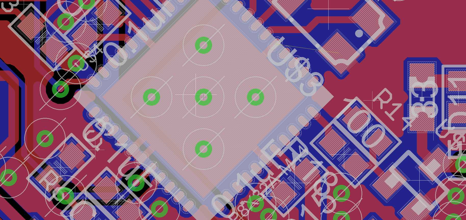
Hey guys, originally I downloaded the eagle library for the propeller that contained the QFN footprint.
I noticed that the center pad was not connected to anything, and I noticed that there was solder mask covering the entire pad. I decided to shrink the center pad slightly, and expose this pad by removing the solder mask.
Is this how this footprint should be done? I'm assuming it should just be connected to ground, and I tossed 5 vias in the center as well. Do people not solder the center pad to anything and leave the solder mask on?
EDIT:
I am also thinking of connecting the corners of the center pad to ground as well... just to get better grounding.
Comments
How are you soldering? Standard IR oven?
https://parallax.com/sites/default/files/downloads/P8X32A-Propeller-Datasheet-v1.4.0_0.pdf
They will be professionally assembled from a PCB assembly company from a pick & place machine, solder paste/stencil, and oven. The challenging part is that I need to solder some prototypes.
Tracy, the diagram you are referring to with the 4 pads... I was under the impression that that is the recommended solder paste stencil to use... not the actual copper layout to use. For example, it seems you have 1 large exposed pad on the PCB, then you put 4 pads of solder paste (generally you don't completely cover the entire pad with solder paste for the reasons you mentioned).
I typically use the QFP chip. This is the first project that had the size constraint so I was required to use the QFN version.
Not to mention supply issues ?
See this post by Ken
http://forums.parallax.com/discussion/comment/1292522/#Comment_1292522
"When these QFNs are gone, they're gone. I'd be happy to be in a shortage situation with QFNs because they move very slow. We will unfortunately EOL this part. The MOQ is too high for the inventory turns we have with them.
If somebody wants to order 12-25K at a time we'll build them; otherwise we can't afford to stock these.
QFNs are not preferred by contract manufacturers due to a lower yield during manufacturing."
What volumes do you expect ?
If it > 12k, or quite small, you may be ok with supply.
Another solution for size is double-sided assembly, or smaller passives, and I've found QFN are not as small as they first appear, when you factor in no-traces under package -> more vias and routing outside the package.
Ken might chime in with a 2017 update on supply chain.... ?
I did have back and forth with the contract manufacturer after initial yield problems. Maybe 8 or 10 out of 100 boards on the first run had problems. Pinpointing issues is time consuming. The CM was experienced, but each new board has its own profile, as much art as science, so that is why you want to do a prototype run to work out the kinks. Another chip on the board, a DFN, was an even bigger problem due to high circuit impedances affected by leakage, but that is all worked out now and I still use that chip, but curse the manufacturer for putting it in DFN in the first place. Multiple problems, troubleshooting headaches. Be sure your CM offers x-ray capability.
As it ended up with the Propeller QFN, the second run reduced the center pad to 285 mil square rather than the 295 mil suggested in the data sheet, and the solder stencil openings were 90 mil instead of 104 mil. The center pad had no solder mask applied. I still don't know if that was a good idea, but the main consideration was to leave plenty of interstices under the chip for pressure washing. No vias, no power dissipation issues. A similar 185 mil pad was on the bottom of the board, connected to distribute Vdd to the 4 Vdd pins with low impedance and act as a very low ESR capacitor.
By the way, your layout looks quite nice. What PCB package are you using?
I don't agree with the fears of using QFNs, especially if you are dealing with a CM because QFNs are old technology nowadays. There really isn't much magic to placing a QFN. The key factor in a DIY field is accurate placement which is a challenge since hobbyists don't have the means for proper inspection/verification (AKA x-ray). Couple that with a lack of good educational data in hobbyist format and you can easily see why so many people shy away from them.
EDIT: Wanted to mention that these dimensions are used with a 5 mil stainless steel stencil. If I was to make a stencil now, it would be 4 mil, but with the same dimensions.
Also you don't have to put designators and values on the silk screen as the parts are just way too small and packed together to do it cleanly. You certainly don't want any silk screen on the pads etc. I just leave these values on mechanical layers so that when I print an overlay of the PCB I print it to fit to the page nice and big and I have these values nice and clear and readable either on paper or on a tablet.
I might have a better footprint to use but I found this and it is a fairly old one that I used successfully at the time and the extra length allows you to get in there and fix up any bad connections.