

USB helper instruction - P2 Possible additional Instructions ???
 Cluso99
Posts: 18,071
Cluso99
Posts: 18,071
Postedit 24May2015:
There is a slight miss-understanding on my part describing the instruction CXORPIN or whatever it ends up being called.
Currently I have a P1V version of this instruction working although not completely tested.
I will post info to the end of this thread.
There is also a CRC instruction helper discussion on this thread
http://forums.parallax.com/showthread.php/151992-CRC-generation?highlight=usb+fs+instruction
At the risk of bullets heading my way, here are a few (simple) additional instructions (using Chip's latest format) that could help immensely...
To aid in bit-banging (reading) USB FS, the following instruction would be an immense help in the tight loop...
ZCL- 1111111 ZC L CCCC DDDDDDDDD xyyyyyyyy CXORPIN [#]D [WZ],[WC]
WC: C = C XOR PIN# where pin# is 0-128
WZ: X = state of PIN#
The above instruction replaces this sequence when bit-banging (reading) USB FS
TEST K,INA WZ
MUXZ NRZI,MASK30
SHL NRZI,#1
To aid in calculating CRC's the following instruction(s) would be a nice help for bit-banging (accumulates 1 input bit only) ...
What we need to achieve for a 1 bit accumulation is basically (please check - this is my current understanding)
(1) The INPUT BIT is XOR'd with the MSB of the CRC
(2) If this result is "1" then the Polynomial is XOR'd into the CRC
(3) The CRC is shifted 1 bit right with the incoming bit from (1) above
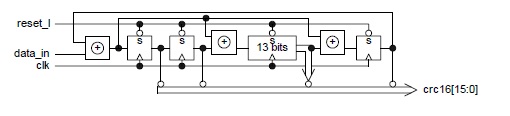
Block Diagram Source: (c)2002 Oguchi R&D (sorry I have lost the link - search google)
I suggest we accumulate the CRC into ACCA or ACCB. This way we can preset the ACCx to zeros or ones (crc variations)
This way we don't need to define a cog long for the CRC accumulation and no other instructions are required.
I suggest the input bit is already in the C flag (because that is how we are accumulating the bit-banging read.
We set a cog long for the Polynomial bits.
Then the single instruction to accumulate each bit into the crc register would become
---- 1111111 nn x CCCC DDDDDDDDD xyyyyyyy0 CRCa D,#n ' accumulate crc into ACCA
---- 1111111 nn x CCCC DDDDDDDDD xyyyyyyy1 CRCa D,#n ' accumulate crc into ACCB
' C=input bit; D=pointer to polynomial; nn= 00=crc5, 01=crc8, 10=crc16, 11=crc32
This gives us the possibility of creating CRC5, CRC8, CRC16 & CRC32.
Just looking for the sequence it replaces now.
The SETRACE instruction is quite powerful.
If we were able to stall the pipe at each instruction if setrace was running it would permit single stepping also
using an input pin to control the stall.
SETRACE could be modified to include this as an option, utilising the next pin# for the input to the "stall" logic".
--RS 1111111 xn L CCCC DDDDDDDDD x11001100 SETRACE D,#0..1 'n=0=no stall, n=1=stall using next pin#
When the stall logic is invoked, it might be preferable for this instruction to take 2 cycles to ensure that another cog can set/reset this pin and this cog sees it???
My misunderstanding - need more coffee
We currently have WAITPEQ (all specified pins one) and WAITPNE (not all specified pins one)
These two would be nice but I cannot see any instruction space available for them
-CRS xxxxxxn nC I CCCC DDDDDDDDD SSSSSSSSS WAITNPEQ D,[#]S,#0..3 'wait for inverted pins equal (ie all specified pins zero)
-CRS xxxxxxn nC I CCCC DDDDDDDDD SSSSSSSSS WAITNPNE D,[#]S,#0..3 'wait for inverted pins not equal (ie not all specified pins zero)
Of course we can possibly invert the pins in the configuration to make WAITPEQ/WAITPNE do this.
There is a slight miss-understanding on my part describing the instruction CXORPIN or whatever it ends up being called.
Currently I have a P1V version of this instruction working although not completely tested.
I will post info to the end of this thread.
There is also a CRC instruction helper discussion on this thread
http://forums.parallax.com/showthread.php/151992-CRC-generation?highlight=usb+fs+instruction
At the risk of bullets heading my way, here are a few (simple) additional instructions (using Chip's latest format) that could help immensely...
To aid in bit-banging (reading) USB FS, the following instruction would be an immense help in the tight loop...
ZCL- 1111111 ZC L CCCC DDDDDDDDD xyyyyyyyy CXORPIN [#]D [WZ],[WC]
WC: C = C XOR PIN# where pin# is 0-128
WZ: X = state of PIN#
The above instruction replaces this sequence when bit-banging (reading) USB FS
TEST K,INA WZ
MUXZ NRZI,MASK30
SHL NRZI,#1
To aid in calculating CRC's the following instruction(s) would be a nice help for bit-banging (accumulates 1 input bit only) ...
What we need to achieve for a 1 bit accumulation is basically (please check - this is my current understanding)
(1) The INPUT BIT is XOR'd with the MSB of the CRC
(2) If this result is "1" then the Polynomial is XOR'd into the CRC
(3) The CRC is shifted 1 bit right with the incoming bit from (1) above
Block Diagram Source: (c)2002 Oguchi R&D (sorry I have lost the link - search google)
I suggest we accumulate the CRC into ACCA or ACCB. This way we can preset the ACCx to zeros or ones (crc variations)
This way we don't need to define a cog long for the CRC accumulation and no other instructions are required.
I suggest the input bit is already in the C flag (because that is how we are accumulating the bit-banging read.
We set a cog long for the Polynomial bits.
Then the single instruction to accumulate each bit into the crc register would become
---- 1111111 nn x CCCC DDDDDDDDD xyyyyyyy0 CRCa D,#n ' accumulate crc into ACCA
---- 1111111 nn x CCCC DDDDDDDDD xyyyyyyy1 CRCa D,#n ' accumulate crc into ACCB
' C=input bit; D=pointer to polynomial; nn= 00=crc5, 01=crc8, 10=crc16, 11=crc32
This gives us the possibility of creating CRC5, CRC8, CRC16 & CRC32.
Just looking for the sequence it replaces now.
The SETRACE instruction is quite powerful.
If we were able to stall the pipe at each instruction if setrace was running it would permit single stepping also
using an input pin to control the stall.
SETRACE could be modified to include this as an option, utilising the next pin# for the input to the "stall" logic".
--RS 1111111 xn L CCCC DDDDDDDDD x11001100 SETRACE D,#0..1 'n=0=no stall, n=1=stall using next pin#
When the stall logic is invoked, it might be preferable for this instruction to take 2 cycles to ensure that another cog can set/reset this pin and this cog sees it???
My misunderstanding - need more coffee
We currently have WAITPEQ (all specified pins one) and WAITPNE (not all specified pins one)
These two would be nice but I cannot see any instruction space available for them
-CRS xxxxxxn nC I CCCC DDDDDDDDD SSSSSSSSS WAITNPEQ D,[#]S,#0..3 'wait for inverted pins equal (ie all specified pins zero)
-CRS xxxxxxn nC I CCCC DDDDDDDDD SSSSSSSSS WAITNPNE D,[#]S,#0..3 'wait for inverted pins not equal (ie not all specified pins zero)
Of course we can possibly invert the pins in the configuration to make WAITPEQ/WAITPNE do this.
Comments
Maybe I can deflect some of the bullets my way!
What would be nice in SETTRACE would be if you could set a specific PC and TASK and every time that PC and TASK are encountered
the lower 32 bits of the system counter are captured to AUX ram.
Being able to measure elapsed time between code cycles would be beneficial in tuning multi-tasking code.
Also automatically stopping SETTRACE when it hits the end of AUX ram.
Another featire that would be beneficial is an addition to the pin transfer function (SETXFR).
If it could be linked to a counter to sample/transmit at a period specified by PHSx values.
Sampling pins at a user defined rate would allow scope like verification of pin activity.
I'll duck for cover now....
Cheers
Brian
LOL! If that were the case, then I think a LOT of us would be in the firing line!
That's not quite correct. WAITPEQ waits for ALL of the masked set of bits (zeros or ones) to match the specified masked PORTx pins, while WAITPNE waits until ANY of the masked bits does not match the corresponding pin. Otherwise, your observation of inverting the test bits would give you your behavior for the two new instructions.
The problem I see with WAITPNE is that you don't know which pin(s) caused the instruction to complete, at least not without querying PINx afterwards. And if the pin in question is toggling quickly (CLKFREQ/2?), you might miss the terminating pin state (i.e. it might have returned to the original state by the time you look at it). I wonder if WAITPNE could be changed to modify the d-field register with the PINx state. Of course, unless the change interval is long, you probably couldn't do much/any processing of the stored value before the pin changes again. This would only really be useful for detecting pulses near the clock frequency, which might be encountered in scenarios like a parallel bus that pulses to indicate a data frame.
But, as you observed, there's no room for more instructions in the format.
That sounds like a very good idea. (but might not be practical)
This would also properly identify a narrow pulse, like from a Counter in carry mode.
GETXP [#]D [WZ],[WC] 'pin into !Z via WZ, xor pin into C via WC (similar to GETP & GETNP)
Just a bit more info for the bit-banging USB FS RX sequence for each bit currently is..
              waitcnt   time, bittime           ' wait for next mid-bit sample time
              test      K, ina          wz      ' read usb pin
              muxz      bits, bitmask   wc      ' b30 (mux mask for rx inbound xor register)
              shl       bits, #1                ' shift new xor'd in bit to b31 (to prev bit)
              test      JK, ina         wz      ' SE0 ? (ie EOP ?)
        if_z  jmp       #waitforend             ' y: wait for end
              rcl       data, #1                ' accumulate bit into data byte
              rcl       stuff, #6       wz      ' accumulate 6 bit blocks. If zero we need to unstuff next bit
[I]'There is no time to accumulate the crc16 here. A special 1bit crc instruction as suggested in the first post would help here.
[/I]   if_z  call      #unstuff
If the special instruction did the following...GETUSB [#]D WZ,WC
where
D = pin no (0..127)
C = C XOR PINx
Z = ! ( PINx OR PINy ) 'ie ZERO if both PINx and PINy are ZERO; PINy = PINx XOR #1
Note1: PINx and PINy are a pair of pins. If PINx is even then PINy := PINx + 1 else if PINx is odd then PINy := PINx - 1
- The allowance for the PINx/PINy pair to be reversed is for USB LS & HS where J/K are effectively swapped between D-/D+.
Note2: WZ & WC could be permanently set on if required.
This instruction would permit the above bit-banging code sequence to be reduced to (replaces 4 instructions)...
              waitcnt   time, bittime           ' wait for next mid-bit sample time
[B]         getusb    K               wz,wc   ' C has prev bit; C = C XOR PIN; Z = !(PIN OR PIN+/-1) = both pin pairs are zero
[/B]   if_z  jmp       #waitforend             ' y: wait for end
              rcl       data, #1                ' accumulate bit into data byte
              rcl       stuff, #6       wz      ' accumulate 6 bit blocks. If zero (6 zero bits) we need to unstuff next bit.
[I]'There is no time to accumulate the crc16 here. A special 1bit crc instruction as suggested in the first post would help here.
[/I]   if_z  call      #unstuff
As you can see, a new single bit 1 clock CRC instruction would help immensely too.
Here is a working USB CRC5 generation for reference...
'initialisation first
              mov       data, xxxxx             ' get the 5bit data
              and       data, #$1F              ' just in case
              mov       count, #5               ' 5 bits
              mov       crc5, xxxxx             ' preset crc5 register
' calculate CRC5
:loop         mov       temp, data              ' get copy of data bits left to process
              xor       temp, crc5              ' lsb of data xor crc5 required below
              shr       temp, #1        wc      ' result of data[lsb] xor crc5[lsb] from above
              shr       data, #1                ' shift input data
              shr       crc5, #1                ' shift crc5
        if_c  xor       crc5, #$14              ' crc5 polynomial =$14=100
              djnz      count, #:loop
Analysing the CRC breakdown for a single bit is (can someone please verify this is correct)...' C has the single data bit to be accumulated into the CRC5 register ' POLY stores the polynomial ' COUNT stores the number of CRC bits in the CRC algorithm rcl temp, temp ' put C into bit 0 xor temp, crc5 ' xor the lowest bit of crc5 and temp, #1 wz ' and put result in Z shr crc5, #1 ' CRC5 >> 1 if_nz xor crc5, poly ' if BIT XOR CRC5[0] = 1 then CRC5 XOR POLYProvided the above is correct then a new special instruction could do the following...(This is slightly different to my proposal for the instruction in the earlier post)
WARNING: There is at least something wrong with the CRC generation below as it does not conform with the block diagram above. Maybe it is just reversed LSB/MSB but I am not sure yet. Can anyone help get this right???
CRCBIT D
where
D = CRCn cog register
C = C has the input bit
and two internal registers POLY and COUNT (set by special instructions, or else ACCA & ACCB could be used) are
POLY = The polynomial (up to 32 bits, unused bits zero) (could be ACCA)
COUNT = The number of bits in the CRC generation (or a mask???) (could be ACCB)
the instruction would perform the following (can someone please check)...
if (C XOR D[0] ) == 1 then
D >> 1
D XOR POLY
else
D>>1
endif
I cannot see the use for the COUNT (number of bits in the CRC) other than at the end of the whole CRC calculation where an AND mask would extract the relevant bits. If this is correct, then COUNT would not be required. What am I missing?
Now the resulting code would become...
[I]'Note: The internal register(s) POLY and COUNT would be previously set as would the users CRCn Register[/I]
              waitcnt   time, bittime           ' wait for next mid-bit sample time
[B]         getusb    K               wz,wc   ' C has prev bit; C = C XOR PIN; Z = !(PIN OR PIN+/-1) = both pin pairs are zero
[/B]   if_z  jmp       #waitforend             ' y: wait for end
              rcl       data, #1                ' accumulate bit into data byte
              rcl       stuff, #6       wz      ' accumulate 6 bit blocks. If zero (6 zero bits) we need to unstuff next bit.
[B]         crcbit    CRC                      ' C has data bit; POLY has polynomial; COUNT (if reqd) has no.of.bits/mask; accumulate the CRC[/B]
        if_z  call      #unstuff
So the new CRCBIT instruction would replace at least 4 instructions.
Chip,
It has been asked before about Re-starting a Cog without downloading new code.
I was wondering what states are preserved (if any) when a cog is stopped. In particular...
When a cog is stopped it draws significantly less current (presumed).
After a cog is stopped, does the cog ram and clut retain their contents?
Are there any registers/counter/etc (PARn, DIRn, etc) that might not retain a valid setting?
The uses for this are to enable the cog(s) to quickly start and perform some support function(s) for other cog(s) and then return to the stopped mode. In order for this to work, the cog(s) need to be able to be started quickly.
An alternative may be a special "SLEEP" instruction that places this cog in a deep sleep (low power) mode, and a special "WAKE #cog" instruction (via another cog) to wake the sleeping cog and continue its' execution.
We of course could use the WAITPEQ instruction and use an internal port pin. I guess it depends on whether more power/current could be saved using alternative methods.
Here is quite a good writeup on CRC generation and various implementations
http://en.wikipedia.org/wiki/Computation_of_cyclic_redundancy_checks
And a good list of the polynomials in use
http://en.wikipedia.org/wiki/Polynomial_representations_of_cyclic_redundancy_checks
Restarting a Cog(s) without reloading (ie SLEEP/WAKE)
ozpropdev/Brian: Yes, I had noticed that. IIRC Chip said the SRAM implementation is static so I am expecting cog ram and clut would remain valid. Not sure about the registers though. I think the most benefit from the sleep/wake method is from power reduction, if it would save a reasonable amount. Otherwise, there are other methods at our disposal to achieve the same result.
I believe I've read somewhere else in those threads, that the Propeller 2 will be a fully static design, working down to zero Hz.
Perhaps in a statement from Chip, but I'm unsure.
So the best way to preserve power, if totaly viable, is selectively 'cutting' a COG's clock source, by the use of some "SLEEP #cog" HUB instruction, issued by itself or by another COG, and afterward 'gating' it again, with some "WAKE #cog", issued by another one.
If controlling a COG in such way, don't mess with the whole silicon die power balance, causing power or clock 'glitches', I'm +1 to this proposal.
But there are some concerns, other than power and clock 'glitches'.
There are so many process that can be running inside a COG, such as the pipeline (and the recent concerns, about upward state backup), counter and serializer blocks, pin circuits, CORDIC and maths.
Orderly pushing their brakes (ABS, EBD, EPS) or a sudden stop?
What happens if each and every active COG, issues a "SLEEP #cog" to stop itself, or, if each one asks for every other to sleep?
Also there is the possibility of a COG issuing a "SLEEP #cog" to another one, just before this one has a chance to issue its own, intended to control the first, or even a third one's behaviour.
Is that possible (or needed) to create a 'NOSLEEP #cog" instruction, to ensure at least one active COG, to remain without disturbance?
Should at least one remain alive, to monitor some 'Dead Man Switch'?
Should a WAKE FROM SLEEP direct connection be provided to each (or every) COG, thru some unclocked external access, other than RESET?
Can a RESET state (other that power on or brown out) be logically differentiated, even by pulse lenght discrimination, to act diversely, in the presence of a (some) SLEEP condition (s)?
I'm sure I couldn't preview all possible scenarios, but the above are the first ones, that arise to me.
Yanomani
I am not certain this is precisely what is required, but it is a reasonable attempt.
By utilising 3 registers and this approximate circuit, I believe we can perform any CRC from 1-32 bits using any polynomial in a single clock cycle.
The polynomial would be written to an internal R/W Register (write is only required). This register could be a new register "POLY" with a new instruction "SETPOLY [#]D" or ACCA could be used.
The number of CRC bits used (eg CRC5, CRC16, CRC32) would be written to an internal R/W Register (write is only required). This register could be a new register "BITS" with a new instruction "SETCRCN [#]D or ACCB could be used.
A cog register would be used to accumulate the CRC register. A new instruction would calculate one bit of the CRC. The input bit would be stored in the C flag. This requires a new instruction "CRCBIT D" that would implement the CRC calculation in a single clock cycle, storing the new CRC back into D.
where
C = current input bit
D = Destination - points to the cog ram register storing the CRC calculation
POLY = an internal register storing the 32 bit polynomial to be used in the CRC calculation (could be ACCA?)
BITS = an internal register storing the number of bits (or a 32-bit mask) to be used in the CRC calculation (could be ACCB?)
The "CRCBIT D" instruction takes the C flag (the input bit) and XORs that with the MSB (determined by the "BITS" register).
If the result is "1" then the
If instead, and internal register was used for the CRC calculation, then it would need to be both R/W as some CRCs require this register to be preset/written with a value.
Currently I have a P1V version of this instruction working although not completely tested.
The C is trying to convey two different states...
1. The current value of the bit received
2. Save the current value of the pin (this is what I forgot about)
Z conveys the state SE0 which is J & K pins =0.
It would also be nice to convey the state SE1 where J & K pins =1.
Currently I have come up with.. My current P1V instruction is in this format and uses one of the available/unused USRx instructions
You will note that my USRx instruction can calculate the CRC16 on the fly in addition to assembling the data byte and unstuffing. By using a normal register I can preset the CRC16 initial value.
I believe that I can use this instruction to keep track of transmitting also, including the stuffing and CRC16 values.
I have left off CRC5 as this seems easy to do in software - to be verified later.
Note that the CRC16 used in USB is not the CCITT version of CRC16 !!!
There is also a CRC instruction helper discussion on this thread
http://forums.parallax.com/showthread.php/151992-CRC-generation?highlight=usb+fs+instruction
I think it's important to keep in mind the overall effect adding special instructions would have, especially if they don't have somewhat broad uses and since it implies that it's something that needs to get added to each cog. So, would a software-heavy approach with helper instructions in each cog end up taking more or less die space than a single minimalist hardware implementation, and what would be the difference in terms of die space and performance between the two options?
My memory on this is hazy but I think there is some additional (seventh) bit stuffed in if you get six zeroes or ones in a row. It'd be good to deal with that in hardware, before crc accumulation etc.
Need to find my usb book where it talks about it
Also, there'll be a meetup down here sometime very soon, if you're interested
I have the unstuffing working and in the middle of verifying the crc16-IBM.
All is done with a single instruction and the returning of the c and z conditions. Each byte is also accumulated.
Does this also manage a Digital PLL somewhere, to maintain bit sampling lock away from the USB edges ?
I have my P1V instruction working. It's not fully tested with all variations but seems to be doing everything desired.
The instruction does unstuffing, calculates crc16 and updates the register, accumulates the data byte, and returns codes. The instruction should be called at the middle of the bit time. This should hopefully allow for a 3 instruction loop to receive each byte.
Next is to try and receive sub data.
I think that is the tricky bit - you can start in the nominal middle, but the bit stuff is there to ensure you have edges to resyc to, as the clocks drift.
USB support may need some state-engine HW (aka DPLL) to keep the sampling "at the middle of the bit time"
Let's continue the USB / Smart Pins discussion here.
forums.parallax.com/discussion/comment/1216080/#Comment_1216080
And here is a nice USB description
beyondlogic.org/usbnutshell/usb3.shtml
Okay. Thanks, Cluso. After I get the USB signaling worked out, we'll have to address all this CRC stuff and make sure we are covered in software.