

P2 Serial / Shift Register discussion
 Cluso99
Posts: 18,071
Cluso99
Posts: 18,071
I thought there should be a new dedicated thread as there are other discussions also going on in the "Big update..." thread
http://forums.parallax.com/showthread.php/150588-Big-update-for-DE2-115-and-DE0-Nano-users-w-add-on-boards/page8
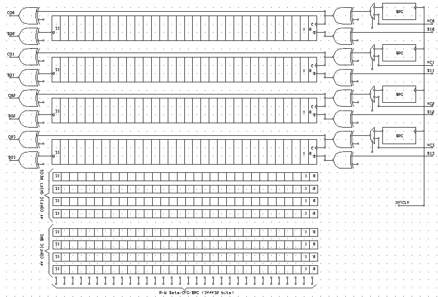
Here is a block diagram for use as a starting point for further discussion...
There are 4 x Shift Registers, 4 x BRGs (Baud Generators), 4 x Configuration registers for the Shift Registers and 4 x Configuration registers for the BRGs. Each can be read/written and are 32 bits each.
Each Shift Register can be used as a Shift In, Shift Out or both Shift In & Out. The Data Input (DI0..3) can each be inverted, the Data Output (DO0..3) can each be inverted, the Clock In can each be Inverted, the Clock Out can be inverted, and the Clock In can each be selected from the Clock Input (XC0..3) or from the Internal Clock divided by the BRG.
http://forums.parallax.com/showthread.php/150588-Big-update-for-DE2-115-and-DE0-Nano-users-w-add-on-boards/page8
Here is a block diagram for use as a starting point for further discussion...
There are 4 x Shift Registers, 4 x BRGs (Baud Generators), 4 x Configuration registers for the Shift Registers and 4 x Configuration registers for the BRGs. Each can be read/written and are 32 bits each.
Each Shift Register can be used as a Shift In, Shift Out or both Shift In & Out. The Data Input (DI0..3) can each be inverted, the Data Output (DO0..3) can each be inverted, the Clock In can each be Inverted, the Clock Out can be inverted, and the Clock In can each be selected from the Clock Input (XC0..3) or from the Internal Clock divided by the BRG.
Comments
...
Shift Register Configuration:
xxxxxxxxx_xxxxx_DDddddddd_SSsssssss
DD = 00 = Data Output Disabled
DD = 01 = -spare-
DD = 10 = Data Output Enabled & Not Inverted
DD = 11 = Data Output Enabled & Inverted
ddddddd = Data Output Pin P0..127
SS = 00 = Data Input Disabled
SS = 01 = -spare-
SS = 10 = Data Input Enabled & Not Inverted
SS = 11 = Data Input Enabled & Inverted
sssssss = Data Input Pin P0..127
xxxxxxxxx_xxxx = currently undefined (we need to work out what modes the Shift Registers can operate)
Clock/Baud Configuration:
nnnn....._xxxx_C_DDddddddd_SSsssssss
DD = 00 = Clock Output Disabled
DD = 01 = -spare-
DD = 10 = Clock Output Enabled & Not Inverted
DD = 11 = Clock Output Enabled & Inverted
ddddddd = Clock Output Pin P0..127
SS = 00 = Clock Input Disabled
SS = 01 = -spare-
SS = 10 = Clock Input Enabled & Not Inverted
SS = 11 = Clock Input Enabled & Inverted
sssssss = Clock Input Pin P0..127 (ignored if internal)
C = 0 = Select BRG as Clock Input
C = 1 = Select Clock Input Pin "sssssss" as Clock Input
NNNN... = Baud Generator (Internal Clock divided by "nnnn.."
Here are some - we need to discuss properly to ensure we don't limit flexibility and overcomplicate the silicon...
- Always LSB first
- MSB can be achieved by REV instruction
- UART 8/32/36 bit with Start/Stop (as Chip has already done)
- 4 bit address option is excellent
- Sync
- Disable auto insert/delete of stop bits
- Specify number of bits 1..32 to tx/rx
- Do we need to be able to read how many bits were read?
- Do we need to specify the data edge to start the shift in on?
- When we write, do we need to be able to restart the clocks, or do we continue at the next clock edge?
- USB
- Use Sync mode above
- Bit Stuffing/Unstuffing by sw
- CRC16 by sw
- SPI
- Use Sync mode above
- Quad SPI
- To do this we need to operate the 4 SRs in parallel and specify the same clock
- Use Sync mode above
- Anything else?
- Mux/shifter to read the bits in correct (or reverse and use REV) order.
- ICS or AC97 ???
- I2C
- Daisy-chain up to 4 shift registers (SRs) (could be done using the internal pins P92..127)
- Work like multiple daisy-chained 74LS595 (without latch)
- Parallel shift register pairs to use one as a data latch???
- When we read a SR do we need to be able to clear/set the SR or clock or clock counter?
- Do we need to count the clocks?
- Could we use the Counters for the BRG instead? (only 2 - is this OK)
- We don't want to limit I/O pins to a groups (except the hw differential pairs)
- Add Mux to input to allow "1" or "0" to be shifted in (permits a stop bit shifted in on underrun, or break)
What have I missed???I don't think it's absolutely necessary, but it could be very nice.
YES, I absolutely think this is necessary.
I think continuing at the next clock edge would suffice.
If there was an easy way to handle /CS strobe in hardware it would be handy. Otherwise software could handle.
I don't think these are necessary. Set / clear could be done by writing back to SR. Not sure about clock or counter.
I think this could be very handy. Might be part of my above statement about /CS?
I think this could be done. I would like the BRGs better though...
I absolutely agree. Any pin, any task.
Seems pretty complete to me, although I'm sure others will have more thoughts.
This first pass lacks an important 9 bit mode. I think 5 bits for bit-frame size, makes this properly flexible.
Uart mode needs to have a Clocked variant. - same bits as classic Async.
[*]Sync
If you have Bit Count field for sync, use that also for Async.
Reading the bits is a good noise-filter. As mentioned before, some SPI slaves check MOD 8 on CLK-Count, before they accept.
This removes one-off impulse noise effects on the CLK line.
It is vital to specify the active edge, otherwise you will be sampling very close to where the data changes.
Transmit usually does not restart CLK (but maybe a Baud-reload, should re-prime to avoid one-more-bit at old rate effects?)
Gapless Send and receive are important, in all modes.
Some slave mode SPI parts, include SS support in the HW, It Gates the Clock (via CE), and tri-states the SPI output.
ie SPI is a 4 pin hardware design exercise.
[*]USB
USB would be nice, but presents a conundrum.
SW only has many compromises and can limit packet sizes, or not fully meet specs - ok for limited tasks, but not commercial.
Bit level HW support is not complex, but needs significant testing time.
Bit-Toggle modulation is really a T-FF, and could be safely made a SPI option.Needs minimal testing.
Edge Sync needs a moderate divide ratio, to give Edge-snap, rather than a pure PLL.
Support of this needs a means to modulate the Baud Divider. Either +1/+0/-1 or pre-load
Bit Stuff / unstuff needs a Gated Counter/state engine, and a Clock Enable on the SPI shifter.
Not large HW, but it needs to be tested.
[*]Quad SPI
Not quite, as that gives 4 shuffled decks - a pain to unshuffle.
I think Chip had worked out how to manage QuadSPI.
The issue is mainly around pin-mapping.
[*]ICS or AC97 ???
This can be done as a SPI variant. It needs the SS pin to have small HW support, of update on BitField End.
(ie not just a SW wiggle but add a single D-FF, or a T-FF.). Probably also a good idea on SPI SS as well.
Who would want to change SS part way thru a field ?
Supposing there Is a rare case, use the Length field, and send t portions.
[*]Could we use the Counters for the BRG ?
Sure, as mentioned before, as a user option. BRG is the default, so the new, smarter and expanded counters are not wasted.
[*]We don't want to limit I/O pins to a groups (except the hw differential pairs)
Whilst this sounds nice, it has a high cost, as you have a LOT of Pin-Map fields.
Mentioned earlier after a Chip discussion, was a pin-follower scheme, where a Pin-map field sets a lead pin, and the others fall into line behind.
Do users really want to scatter their SPI pins all over the device ?
Lol, I also note the data is note arranged serially. Except for command compatibility, Quad-SPI is really a 4-bit parallel port. That's gonna be a hassle to re-package the data to and from the shift registers. It might actually be faster to bit-bang it!
These are very good questions. My experience with the P1 and QSPI was a bit annoying just because of the bi-directional pins. I have all but given up using counters to run the clock due to timing restrictions. You are also very right about re-packaging the data to and from shift registers. Bit banging may be the way to go.
My interest for USB is simple devices such as keyboard and mouse. FLASH drives would be a great addition but not entirely necessary.
There was a previous comment suggesting this was largely fleshed out.
Not that much more complex, just follow the rule of Bit-level in HW and Byte/word level in SW.
No, you just build the shift register with muxes. It shifts nibbles, but reads / writes in parallel, as 32 bits, with the bits in the correct places.
I have yet to find an example of how the hardware handles transforming between the various serial and parallel modes.
I absolutely agree. Any pin, any task.
.[/QUOTE]
average joe seems to be doing pretty much exactly the same things I am. I can't add much except to highlight free pin assignments. I don't know about everyone else, but my pin assignments constantly change until the board layout is finished. I will happily update my code and schematic to get rid of a via or two!
This seems overly complicated to me..... in fact I can't even follow your proposal without studying it more than I'm prepared to do at this time.
I'd be happy with 4 cascadable registers, each double buffered with an auto-transfer after N clocks so the driving software can continuously feed/read data at jittery intervals. I simply wish to be able to continuously stream data perfectly, and have time to analyze data (CRC, LFSR,CHECKSUM,BOSE-CHAUDRY, etc) while streaming is ongoing. Also, it would be nice (but not imperative) if the clock generator could also employ a "swallow" mode like radio RF generators so any frequency could be made, not just integer-divides of the clock.
Just my opinion.
Cheers,
Peter (pjv)
I agree that buffering is needed to get the most benefit from the shifters.
Chris Wardell
No, it is not ordinary, it has muxes added.
That changes the hand-over points, so each bit reaches 4 ahead, and the last 4 (or first 4) drive the IO pins.
8 clocks move all 32 bits, but it reads as a 32 bit register
- this is a couple of lines in HDL.
Expanding:
This simple control-pin option of a D/T FF, (Bit-frame clocked, so control pin is exactly known) should also be available in all Async modes, where it would be very useful for RS485 direction handling.
I think I got it. Only one of the four 32 bit buffer registers gets used.
The special case wiring for Quad-SPI is stacking up.
I know ... that's a bit snarky. It's just I'm finding myself a bit shocked at how non-SPI it is. It's a bit rude to have a related name.
Not really, it is a nibble wide super set, designed to still fit into 8 pin standard packages.
Most (all?) QuadSPI parts can still run 1-bit SPI mode, and to make it nibble wide, you have to go bi-directional.
So there will be caveats, but nothing some simple HW cannot accommodate.
Then there is DDR QuadSPI ....
- because the Prop 2 is likely to be pin-bound ~ 50MHz pin wiggle, DDR has appeal, and starts to make XIP more compelling.
More important, is to look at a device like Spansion S25FL128SA, available for under $2, and see how the QuadSPI DDR works.
It does not look too bad,
4.2.1 shows a 1-bit SPI command sent, then 32 bits of Address, then Mode of 8 bits, left justified in 32 bits (24 bits dummy) and then Data follows after a turn around time.
Figure 10.52 Continuous DDR Quad I/O Read Subsequent Access (4-byte Address, EHPLC=01b)
gives clearer info on the turn around.
32 bits of Address. DDR
8 bits of mode
24 bits of floating IO (3 full clks at DDR = 6 slots = 24 bits )
then the Flash device emits 32 bits of DLP, and then Data streams.
If you wanted to software-assist this, you need length control in 4 bit multiples (fits inside the proposed 1 bit granularity)
and a Dirn bit on TriState, that can be bit-Frame sync'd
From Figure 10.52 Sw actions are then just this :
Length=32, TxMode(drive pins) Send Address. [4 clocks]
Length=8, TxMode(drive pins) Send Mode [1 clock]
Length=24, RxMode(Float pins) Discard RX data [3 clocks]
Length=32 (DLP size), RxMode(Float pins) Discard RX data [4 clocks]
(adjust these Float+Discard phases, in SW, to suit vendor or chip changes )
and after the above 12 clocks setting address and chip getting ready, then valid read data streams from Flash
repeat for as much data as you want ...
Length=UserChoice, RxMode(Float pins) Vaild RX data [Length/8 Clocks]
Note that continuous DDR skips the 1-bit command preamble, so has a 'sticky' command, but drops the clocks needed.
Again we follow the rule, HW-does-bits, SW-does-bytes.
Sorry if you are not understanding me. I am not trying to make it overly complex, just extremely flexible, with all shift registers being identical.
What parts don't you understand? - my fault if you don't follow, so please ask.
I would love to ask for a CRC16 instruction but am not game to ask. This is one of the problems with FS USB. Without a shift register, FS is proving to be quite difficult at 80MHz but I think I will eventually get there.
This becomes semantics, one mans divider can be another mans counter.
Most modern BRG are reloadable dividers/counters, so they are not binary, but /N.
because RX needs to do a half-bit offset, there usually is an 'Even N' implied so the formula Fb = FSys/(2*N)
Next, practical Async sample-width/jitter considerations usually have N > 2, but a CLK-OUT Async mode could support FSys/2,
up to the pin-limit.
I prefer baud formula. to words. Makes it very clear what is supported.
In RS485. many modern UARTS now have a RS485 direction bit.
This changes at the exact end of the Stop bit, so the BUS Transceiver flips direction. (half duplex)
In SPI, SS-Pin control is best bit-Frame aligned, this just extends that option, to Async, to support the RS485.DIR pin.
- We can free up a whole instruction and perhaps this should be the WTG.
- The R bit indicates read or write
- Regarding clocking etc, I wondered if all instructions should be 2 clocks.
- If the instruction read/writes the shift register while a shift clock executes, then the instruction read/writes again on the next clock, else the clock is just a nop stall. Keeps timing deterministic.
- Regarding Q-SPI, read/write of data effectively goes thru a barrel shifter (think that's the correct term). D0-3 have to go to separate shift registers for D0, etc. Same applies to read. Others may refer this as muxing. We only need to be able to explain what is required and Chip will understand.
Seems to me that none of this is likely to work with multi-threads and super fast I/O. I am basing this on the USB FS that I am working on.Currently all I am trying to do is monitor the FS data. I am not getting enough time to get it going yet.
Software is doing the bulk - see
Length=32, TxMode(drive pins) Send Address. [4 clocks]
Length=8, TxMode(drive pins) Send Mode [1 clock]
Length=24, RxMode(Float pins) Discard RX data [3 clocks]
Length=32 (DLP size), RxMode(Float pins) Discard RX data [4 clocks]
Length=UserChoice, RxMode(Float pins) Vaild RX data [Length/8 Clocks]
The HW is minimal, - a couple of lines of HDL to morph shifter to Quad compatible, (it reads/writes bit-correct, no shuffles needed)
and even DDR is not complex if you have a higher SysClk, which P2 does.
To me the pin-mapping is the more complex issue, but I think Chip had that covered.
in DDR, standard Shifter clocks from faster internal CLK, and that toggles a pin, for the slower DDR clk. (master mode)
Some Tpd care would be needed, to phase the CLK pin and Data (this could be Data from a other-edge FF, at SysClk speeds)
The Spansion part specs 66MHz DDR.Quad, so depending on the Prop 2 pins I'd guess 50~66MHz nibble rate.