

Video graphics controller using Propeller to control SDRAM

So for a while now I've been looking into the possibility of using the Prop's video hardware to drive not
the data but the control signals of an SDRAM, allowing operation near or at the full design speed as a
video RAM, and also for signal capture (logic analyser, digital scope).
I designed a simple breakout board for a generic 54 pin SDRAM (SDR, PC100 or PC133). When this came
back from the PCB fab I got out the trusty sandwich toaster (converted to reflow oven) and transplanted a
HY57V56820B SDRAM chip onto it and started experimenting in earnest.
I'd previously written various pieces of PASM for driving various SDRAM functions and checked the timing
on the scope, to get basic confidence it was feasible.
Currently the setup is using the Prop clock / 4 as the SDRAM clock, but the technique can go faster, you just
have to insert NOPs in the SDRAM instruction stream (provided by the video hardware) so that you can
update the address bus faster enough (typically with consecutive "mov OUTA, addr" instructions.
So for each set of SDRAM instructions to send I have to choose a subset of at most 4 instructions, put their
pinstates into each of the 4 bytes of the colours argument to waitvid, and a set of di-bit selectors is fed as the
pixel data. A pin driven by CTRA both clocks the LCD and the SDRAM clock, and the low Prop
pins are connected to the address and bank-select lines.
For generating video to an LCD screen I use page-mode burst reads, setup at the start of the scanline (one
of the pins waitvid is controlling is the DEN pin on the LCD (it has DCLK/DEN + 18bit colour inputs - no HS/VS
to worry about) so that this can be set high two cycles after the READ instruction is issued (I'm using a CAS
latency of two).
waitvid is used to feed nops (and keep DEN high) for 800 cycles, then a different waitvid clocks in a BURST-TERM
instruction followed by PRECHARGE to close the row.
Between scanlines 4 AUTO-REFRESHs are issued to keep the DRAM happy, and at the end of the frame (480 lines)
I use a big gap of 100 scanlines to switch to code that writes the DRAM.
I push records onto a queue in hub ram, each represents a horizontal line segment to paint, its x, y coords and pixel
width and colour. During the 100 blank lines time the same cog pulls these off and executes burst-writes to update
the SDRAM with the updates, whilest keeping a count-down cycle counter updated with the number of video clocks
passing. When close to the deadline the code vidwaits for the actual deadline and goes back to the screen display
code.
Anyway, time for images and videos:
http://www.youtube.com/watch?v=4E17x2Piqw0
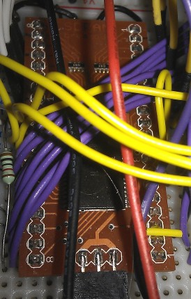
The breakout board is hard to see with all the connections! The actual SDRAM I have has 8 data pins used, not the full 16 that
the 54 pin package allows, and these are routed straight to some of the colour pins on the LCD flex-pcb breakout. I've also added
resistors between some of the lower address pins and the datapins to allow the address bus to be used to write values to the RAM.
For graphics I'm setting up one value to the data pins (via the address pin resistors) and burst writing it to the whole line-segment
drawn, so the speed of Prop I/O isn't limiting the datarate.
In theory with a well laid out PCB and perhaps replacing the resistors with a DQ latch it would be possible to go upto 80MHz
clocking.
My next experiments are going to be generating 1024 x 600 (WSVGA) at 40MHz pixel clock. This is 1024x768 with more blank
lines (to enable more graphics painting).
The current SDRAMs I have on various DIMMS are mainly 32MB so will hold over 50 screenfuls at WSVGA resolution. This would
enable frame-by-frame animation of course") The video shows that vertical hardware scrolling is trivial, only the row-address has to be
The video shows that vertical hardware scrolling is trivial, only the row-address has to be
updated - the driver already reads this from hub ram.
The test patterns are generated in Spin using the sine table and are written to 4 screenfuls of memory (after having overwritten all 68
screenfuls at start up).
[edit: BTW the LCD is a CLAA070VA01 from a recycled Phillips digital photo frame,
it has a relatively sane interface, all 3.3V, just DCLK/DEN and 18 bit digital colour
http://www.beyondinfinite.com/lcd/Library/Chungwa/CLAA070VA01.pdf ]
the data but the control signals of an SDRAM, allowing operation near or at the full design speed as a
video RAM, and also for signal capture (logic analyser, digital scope).
I designed a simple breakout board for a generic 54 pin SDRAM (SDR, PC100 or PC133). When this came
back from the PCB fab I got out the trusty sandwich toaster (converted to reflow oven) and transplanted a
HY57V56820B SDRAM chip onto it and started experimenting in earnest.
I'd previously written various pieces of PASM for driving various SDRAM functions and checked the timing
on the scope, to get basic confidence it was feasible.
Currently the setup is using the Prop clock / 4 as the SDRAM clock, but the technique can go faster, you just
have to insert NOPs in the SDRAM instruction stream (provided by the video hardware) so that you can
update the address bus faster enough (typically with consecutive "mov OUTA, addr" instructions.
So for each set of SDRAM instructions to send I have to choose a subset of at most 4 instructions, put their
pinstates into each of the 4 bytes of the colours argument to waitvid, and a set of di-bit selectors is fed as the
pixel data. A pin driven by CTRA both clocks the LCD and the SDRAM clock, and the low Prop
pins are connected to the address and bank-select lines.
For generating video to an LCD screen I use page-mode burst reads, setup at the start of the scanline (one
of the pins waitvid is controlling is the DEN pin on the LCD (it has DCLK/DEN + 18bit colour inputs - no HS/VS
to worry about) so that this can be set high two cycles after the READ instruction is issued (I'm using a CAS
latency of two).
waitvid is used to feed nops (and keep DEN high) for 800 cycles, then a different waitvid clocks in a BURST-TERM
instruction followed by PRECHARGE to close the row.
Between scanlines 4 AUTO-REFRESHs are issued to keep the DRAM happy, and at the end of the frame (480 lines)
I use a big gap of 100 scanlines to switch to code that writes the DRAM.
I push records onto a queue in hub ram, each represents a horizontal line segment to paint, its x, y coords and pixel
width and colour. During the 100 blank lines time the same cog pulls these off and executes burst-writes to update
the SDRAM with the updates, whilest keeping a count-down cycle counter updated with the number of video clocks
passing. When close to the deadline the code vidwaits for the actual deadline and goes back to the screen display
code.
Anyway, time for images and videos:
http://www.youtube.com/watch?v=4E17x2Piqw0
The breakout board is hard to see with all the connections! The actual SDRAM I have has 8 data pins used, not the full 16 that
the 54 pin package allows, and these are routed straight to some of the colour pins on the LCD flex-pcb breakout. I've also added
resistors between some of the lower address pins and the datapins to allow the address bus to be used to write values to the RAM.
For graphics I'm setting up one value to the data pins (via the address pin resistors) and burst writing it to the whole line-segment
drawn, so the speed of Prop I/O isn't limiting the datarate.
In theory with a well laid out PCB and perhaps replacing the resistors with a DQ latch it would be possible to go upto 80MHz
clocking.
My next experiments are going to be generating 1024 x 600 (WSVGA) at 40MHz pixel clock. This is 1024x768 with more blank
lines (to enable more graphics painting).
The current SDRAMs I have on various DIMMS are mainly 32MB so will hold over 50 screenfuls at WSVGA resolution. This would
enable frame-by-frame animation of course
updated - the driver already reads this from hub ram.
The test patterns are generated in Spin using the sine table and are written to 4 screenfuls of memory (after having overwritten all 68
screenfuls at start up).
[edit: BTW the LCD is a CLAA070VA01 from a recycled Phillips digital photo frame,
it has a relatively sane interface, all 3.3V, just DCLK/DEN and 18 bit digital colour
http://www.beyondinfinite.com/lcd/Library/Chungwa/CLAA070VA01.pdf ]
Comments
-Phil
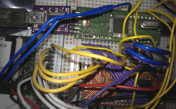
a 16374 latch to drive the data-bus from the address-bus rather than resistors. Its all datapath... The connector on the
right is for a different LCD it happens, one from a cheap calendar/photo frame from Maplin here in the UK, but I haven't
fully reverse engineered it yet [ and its glued into its enclosure
So I feed P0..P12 to A0..A12, P13-14 to the bank address bits, and P0..P15 also go to the latch. Most of the control signals
for the SDRAM and the latch come from P16..P23 under the control of waitvid, and a few others come out on P24..P27
I've changed the demo mode to just draw random circles as fast as possible (given that Bressenham's is coded in Spin), see
video:
And finally the initial code, untidy though it may be:
A little while backed I looked at using 8 of the newer 4-bit mode SRAM chips from microchip to do something vaguely similar, but your solution is much better. It will also help to bridge the gap between p1 and p2
how to drive them without too much anxiliary logic such as counters - SDRAM's page burst mode
is so handy.
http://en.wikipedia.org/wiki/SDRAM#SDR_SDRAM
In theory (not yet tested) you can drive multiple banks to give a single uninterrupted scanline, meaning the
screen width can be more than the column address range. Many chips have 9 or 10
bit column addresses, giving upto 1024x768 as resolution.
The 16 data bit chips have narrower column addresses usually (9 bits) they should be found
on SODIMMs rather than DIMMs I believe, yet to get some.
SGRAMs would be even better (block and masked writes, 32 bit databus), except they are
mainly low capacity and you might need a whole stick of them (SODIMM's worth) to drive
a whole screen. You'd also need another control bit.
during writes, tested a different brand of SDRAM (micron) and changed to using the ROM
font. Also fixed a few issues with special-case code for painting short spans.
Am working on polygon-render PASM code to live in another cog, converting vertex list to pixel
spans.
I was fairly certain that color data bits could be sent directly to an LCD panel without the timing constraints imposed by typical video sync signals, and that an SDRAM chip contained most of the circuitry required to scan and present the data for an LCD panel to display. This would make a good display subsystem for many applications.
I can see how you could use the video generator to produce 6 control signals, but how are the other 5 control signals generated?
Firstly I have a TFT display that doesn't need Hsync or Vsync, so I only need to generate DEN signal synchronously for it, leaving 7
other video pins.
SDRAM has nCS, CE, nRAS, nCAS, nWR and DQM to drive it (arguably the nCS and CE can be separately done as they only need to change
at init time if you aren't going to use low-power self-refresh. DQM you only need for masked writes (such as glyphs with transparent
background). The rest is address and data (bank select is just a special kind of address pin) which do not need to be synchronous as
they are only sampled by specific SDRAM opcodes and you just make sure they are setup early enough by trial/error. It wouldn't be
hard to add DQ-latches to the address lines to syncronize if you wanted - I already use such latches to gate address pins onto data pins
for writing (one of the video pins drives the nOE of the latch).
Yes, I know. I was involved in a thread that discussed using recycled TFT displays with the propeller when I first joined the forum. That was when I became fairly certain that most bare TFT displays did not need Hsync or Vsync, only a clock, data (color), and enable/reset signals. That also made the signal timing less critical.
Thanks for the quick reply Mark. I should have been more specific. I was not really thinking of the P0 – P15 signals when I asked. The use of those are fairly obvious. I was looking at the signals produced by P16 to P26 on the propeller.
I realize the DEN for the TFT and the /CS & CKE for the SDRAM can be set at init time but doesn't the TFT DCLK have to be synchronized with the data read from the SDRAM, and the LE & LCLK synchronized with the data written by the propeller?
Can you describe how this is done?
them on separate pins, thinking that would generate faster edges than distributing one pin
to both devices. P0..P12 are address bits, P13/P14 are bank select, P15 SDRAM clock,
P16..P23 video pins, P24 is TFT DCLK, P25 clocks the address->data latch (done asynchronously).
2 pins spare.
Currently the video pins are DEN/CE/nCS/nRAS/nCAS/nWR/LE/DQM, where DEN is for TFT, LE is
output enable on the latch, the rest are SDRAM pins.
For a display needing Hsync/Vsync I think a separate cog just to generate those signals would
be the easiest approach since the SDRAM cog has to do writes during vertical blanking.
My idea for a complete graphics subsystem is:
serial cog - reads instructions from serial pins and enqueues commands for the system
polygon cog - interprets polygon instructions into span lists queued for the main SDRAM cog
SDRAM cog, drives display and writes to SDRAM during vertical blank time (spans and glyphs),
also auto-refreshes during H-blanking
[ optional timing cog to handle H-sync/V-sync ]
I'd like there to be a few more pins spare really, could then have an SPI bus to talk to a touchscreen
or SDcard. Extended I2C EEPROM could hold some extra fonts though, that would be straightforward.
By reducing the address pin count more pins can be freed though... 32MB is more than enough for a
frame buffer. The SDRAMs I've experimented with so far are Hynix HY57V56820BTH and Micron
MT28LC16M8A2 (both 4 banks x 8M x 8bit). I'd like to find a 16 bit SDRAM too to give 16 bit colour
without needing two chips.
so the sdram ops get spaced further apart (cyclewise) to allow the writes to OUTA to keep up.
My TFT panel (800x480) seems to cope at 40MHz (its spec'd for 25MHz to 50MHz) but not at 50MHz.
Actually its a bit flaky without a groundplane but I plan a PCB in the next few weeks to improve RF
behaviour.
(with a breadboarded setup I'm not at all surprised about 50MHz failing, the TFT DCLK signal is
travelling 5 inches in free space to the flex connector then another 4 inches along it! Impedance
mismatch city).
By halving the clock to the TFT but not the sdram I've verified the sdram is functioning correctly at
50MHz (you get horizontally squashed graphics!) Even the 74HC374 latch seems to hold up (though
I'm only really hammering the output-enable on it). Future versions will use 74LCX and groundplane,
hoping for 80MHz...
There has been some tidying of the code, mainly in defining all the sdram opcodes symbolically to make it
easy to change pin assignments in the future. [latest version attached]
I'm designing a motherboard/daughterboard system for the system, with 2 sdrams to give 16 bit
colour (most sdrams on dimms are 8 bit, its what I have for free!). In theory it should be able
to drive something like 1024x600 or 1024x768 standard VGA, but we will see. Other daughterboard
options might be 18 bit lvds
I also tried some code to switch seamlessly from a read-burst on one bank to another - this works and
thus the sdram page size needn't be 1024, a 512 or 256 page size could be used (assuming more than one
bank). Or drive 1920x1080
There are commented out versions of burst_read routine in there.
[ also, got a new video uploaded:
The main board has 2 SDRAMs allowing 16 bit colour, using 32M chips so 64M in total.
Propeller, EEPROM and a 74LCX16374 latch form the rest of the circuit, satellite board
on a 15x2 header handles the specific output device, currently still my 800x480 LCD.
VGA and LVDS next in the pipeline.
Pin assignments changed slightly (SDRAM clock moved from pin 15 to allow full 16 bits
for colour.
More software additions include clipping to rectangle in the graphics primitives, and setting
a frame buffer page (for the 800x480 screen I get 64 pages as the screen is just under 1M.
Currently the Bressenhams line drawing is in Spin so its noticeable slower than circles, polygons,
rectangles, text!
Video here:http://www.youtube.com/watch?v=P-TxY1nGczA
I have an idea how hard this is having breadboarded something last year and not getting it to work fast enough. And yet here you have a video showing it doing some very nice graphics.
Thinking ahead, this could be a fantastic standalone graphics board. How many pins do you have free on the propeller, and what would be the best way to talk to such a board? (eg 2 wire RS232, or 3 wire SPI slave etc).
signals to give a return path to the high-speed clocks. Ideally this would be a 4-layer board but its a compromise (2-layers, as much
groundplane on either side as I can get). I do like the richness of 16bit colour, such a difference..
I am running out of pins, it is true - I think I'll just be using the RX line to receive serial commands - the TX line is currently shared with VS
for displays that need it (not tested yet). However the data clock might perhaps be borrowed for standard VGA which doesn't need explicit
dot-clock. And I have 4 cogs to spare I think.
Data: 16 (shared with 15 address and bank-address lines)
SDRAM cloack & control signals: 7
DEN, write-latch clock, write-latch-enable: 3
DCLK: 1
So 27 used before considering Hsync and Vsync. However I could perhaps share RAM clock and dot clock, and permanently
wire the clock-enable pin of the SDRAMs.... Going down to 15 bit colour frees a pin too.
Board schematic and layout:
[edit: just to add that I now have an LVDS TFT screen working now, LTN101NT02 10.1 inch WSVGA (1024x600),
using a DS90CF363 LVDS encoder chip. It turns out to just need DEN, not HS/VS, so it was 'easy'. Am running it
at 50MHz dot clock and about 60fps.]
[edit: photos of 10" screen:]