

Ground Plane / Copper Pour around SX/ADC
 VonSzarvas
Posts: 3,634
VonSzarvas
Posts: 3,634
Hello all,
I am nearing the end of my project*, and am now thinking about PCB layout.
In short: Any tips on any gotchas and must-do's when laying out a pcb containing power (DCDC SIL), SX chip and an ADC circuit most welcomed.
In Long:
I have read some seemingly conflicting ideas about what is best when laying out pcbs containing digitial and analog devices. Although the most articles seem to agree on the following:
1. Must layout in this order: Power, Digital, Analog.
2. Lay a solid (as possible) ground plane on back of pcb.
3. If needed, create a ground plane island around the analog section, but ensure a bridge is linking it to the main ground plane so that traces do not need to cross a broken ground plane.
4. When routing power and ground, keep them together - so as not to create a loop with a large gap between. - mostly eradicated by a ground plane I guess...
5. Do not route analog traces under digital ones, or digital ones under analog.
And now the perhaps more contentious points....
6. Do NOT lay a ground plane under the resonator or crystal, or its wires connecting to the SX chip ? Is this true- as on the parallax supplied sx28 prototype boards this has not been done.
7. My understanding is the copper pour is copper poured into "unused" areas of the pcb face. The copper pour effectively becomes a ground plane if you attach the copper-pour to all the gnd/vss points in the circuit.
8. I really don't understand if I should be using a copper-pour/ground plane on just the bottom of the double-sided pcb, or on both sides. Or perhaps ground-plane on the bottom and just unconnected copper pour on the top...
Thanks for reading!
Max.
Notes:
a) As a reference, I found this article very interesting: www.hottconsultants.com/techtips/split-gnd-plane.html
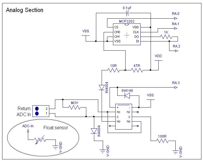
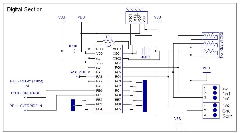
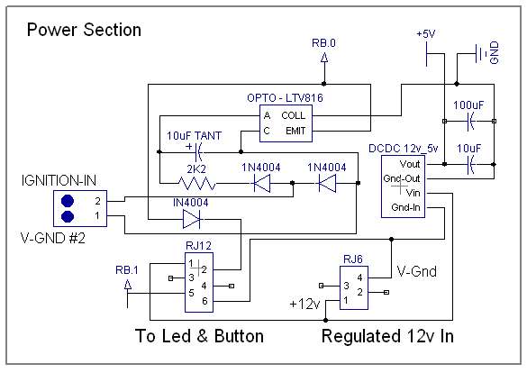
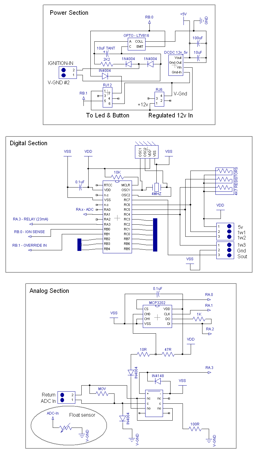
b) I also have attached my schematic, which may prove of interest to someone! It it not too well elaborated yet, but if somebody has a question please do not hesitate!
c) * Project is to create a kind of interface to a fish tank level alarm. Currently it lights some indicators and alerts if the water level moves into/out of certain preset levels. My aim is to "intercept " the signal when the vehicle is parking and monitor the level (and also temperatures using a couple of 1-wire sensors). During this time, a relay shunts the existing device to GND via a 100R resistor to make it think all is well and not set off an alert (annoying beeping). Later (phase 2) of the project will add a data logger. Then, we can get the data back at the end of each period and see whats been going on.

Edited: Schematics updated and split into sections so can be more readable.
Post Edited (Maxwin) : 11/18/2007 12:18:42 PM GMT
I am nearing the end of my project*, and am now thinking about PCB layout.
In short: Any tips on any gotchas and must-do's when laying out a pcb containing power (DCDC SIL), SX chip and an ADC circuit most welcomed.
In Long:
I have read some seemingly conflicting ideas about what is best when laying out pcbs containing digitial and analog devices. Although the most articles seem to agree on the following:
1. Must layout in this order: Power, Digital, Analog.
2. Lay a solid (as possible) ground plane on back of pcb.
3. If needed, create a ground plane island around the analog section, but ensure a bridge is linking it to the main ground plane so that traces do not need to cross a broken ground plane.
4. When routing power and ground, keep them together - so as not to create a loop with a large gap between. - mostly eradicated by a ground plane I guess...
5. Do not route analog traces under digital ones, or digital ones under analog.
And now the perhaps more contentious points....
6. Do NOT lay a ground plane under the resonator or crystal, or its wires connecting to the SX chip ? Is this true- as on the parallax supplied sx28 prototype boards this has not been done.
7. My understanding is the copper pour is copper poured into "unused" areas of the pcb face. The copper pour effectively becomes a ground plane if you attach the copper-pour to all the gnd/vss points in the circuit.
8. I really don't understand if I should be using a copper-pour/ground plane on just the bottom of the double-sided pcb, or on both sides. Or perhaps ground-plane on the bottom and just unconnected copper pour on the top...
Thanks for reading!
Max.
Notes:
a) As a reference, I found this article very interesting: www.hottconsultants.com/techtips/split-gnd-plane.html
b) I also have attached my schematic, which may prove of interest to someone! It it not too well elaborated yet, but if somebody has a question please do not hesitate!
c) * Project is to create a kind of interface to a fish tank level alarm. Currently it lights some indicators and alerts if the water level moves into/out of certain preset levels. My aim is to "intercept " the signal when the vehicle is parking and monitor the level (and also temperatures using a couple of 1-wire sensors). During this time, a relay shunts the existing device to GND via a 100R resistor to make it think all is well and not set off an alert (annoying beeping). Later (phase 2) of the project will add a data logger. Then, we can get the data back at the end of each period and see whats been going on.
Edited: Schematics updated and split into sections so can be more readable.
Post Edited (Maxwin) : 11/18/2007 12:18:42 PM GMT
713 x 563 - 37K
841 x 467 - 45K
585 x 414 - 31K
853 x 1497 - 80K
Comments
Can you actually read the schematic image you posted? For once I find myself suggesting that someone post an image that is larger. At 891 X 631 your schematic image is basically unreadable as is. Also, light gray letters on white are really hard to read.
Thanks,
PeterM
I have updated the original schematics to include separate files for the 3 sections, as I think it was too much on 1 page causing the main problem. I also included all 3 together in the last file, if someone prefers that and has a larger monitor with zoom.
Board moderator: It occurred to me this post may be more appropriate in the Sandbox, as not entirely an SX question, but rather a more generic topic for all Parallax chips. If you do move it, I will update the title appropriately.
Max.
Post Edited (Maxwin) : 11/18/2007 8:37:11 PM GMT
I have attached my first ever pcb design, based on the earlier schematic! Yippee!
Any feedback would be great. In particular, my earlier concerns which in short are:
1. I have added a ground plane/copper pour on the bottom layer, connecting all the VSS points. Is it sensible to do the same on the top layer? Or alternatively just put in a pour on the top which is not connected to ground? Does it make a difference?
2. The break in the ground plane around the analog section... is it worth it, a waste of time, likely to cause more problems than it solves... ?
3. I have not done so yet, but as I have read commented, is it really worth to remove the ground plane from under the resonator - or is that just myth/not relevant for the SX?
4. Is it sensible to "tie" the vehicle ground and 5v gnd together (as I have done). I have tried to isolate noise coming from the ignition sense (opto device), by giving that its own earth connection (Vgnd#2), but for the ADC circuit I figured I would rely on the vehicle ground being in my circuit anyhow, so by connecting the 2 together at the DCDC converter, I figured I may be saving myself some ground loop trouble.
5. Any other obvious clangers ?
Thanks for looking, Max.
Admission: I appreciate I have mounted a couple of components "the wrong way round" according to the others on the pcb, but overall pcb size and short track length were my prime concerns here, rather than ensuring no placement errors are made in mass-production. I am sure given more time I can rework the jigsaw and find a completely consistent way, but this will serve the purpose for my first effort. Actually really enjoying putting these together - beats crosswords!
Notes: The markings on the side of the SX-Key socket next to the resonator are just to tell me which way round to plug in the key! The headers connecting to the unused pins on the SX are just in case I want to add something later. I figured I can just pull the pins high until I need them later.
1. All components facing same way.
2. Power section now moved far away from analog.
3. No longer need any vias!
Just a problem with the drawing program, getting the copper-pour perfectly angled, but working on that.
Unless anyone has any input, I think I will get the pcb made with copper-pour connected to ground on both sides, as my latest Parallax boards follow that method. And I won't remove the copper-pour from under the resonator as again my Parallax prototype boards have not done that. I will soon fine out if ADC circuits don't like this!
I noticed 100uF capacitors. I recently got miniature 100uF/16V electrolyt capacitors
(low profile) but these were 6mm in diameter and the smallest I could find.
If you have 100uF capacitors that fit your design, can you provide
an ordernumber from where you got them?
regards peter
The provision for capacitors around the psu were added "just in case" - and so there is the lesson learned not to do that without checking sizes. (I did not add anything else just in-case, thankfully, and have just printed out the pcb on paper again to ensure all other components fit).
Actually I did not have component values in mind, as the datasheet from the manufacturer of the dcdc convertor just recommends Cin and Cout without values, so I thought I would need to experiment once the pcb arrives - without paying attention to possible size issues. I am thinking about adjusting the layout so that a small ceramic type cap and a larger electrolytic cap could potentially fit each side of the dcdc.
The 12v supply is actually coming from a filtered and regulated ups device, so I would not expect to many issues on the 12v-in side of the dcdc... although you never know..
Much better schematic images now.
Most of my thoughts have to do with the silkscreen layer. I'm assuming your board will have one, since that green on the top layer appears to be the silkscreen superimposed. Even if you don't, you can always put text on the top (and bottom) copper layers. Anyway, it's good that you put some orientation marks on the board to know which way to plug in your SX. You might consider going even further. I always have something like "SX Back" or "SX Top" to let me know which side of the header pins has which side of the SX-Key. I try to keep it idiot proof.
Another thing that helps is to add a single pin header for ground, or a two pin header for ground and your 5v section. These can be anywhere on the board that is simple for your layout. This is useful when you're trying to check things out on the board. Having a simple, dedicated place to clip a ground lead on (or grab 5 volts) can make things much easier when debugging hardware. Make sure they are labeled.
Finally, consider adding some labels to the header you have on the board. I'm not sure what pins they connect to without looking at a datasheet. It's a lot easier to have them labeled "PA1 PA2" or "B3 B4" (or whatever pins they are) then having nothing. When you need to use them, you'll find it's nice and quick to have labels on them. You might also consider adding two more pins (5v and ground) to the header strip so they are there in case you need them for any add-on parts.
Thanks,
PeterM
About the SX-Key though, I will keep that as is. I think everyone has a preference, but for me (and its only me building this thing for fun), the hash marks on one side (meaning not the flat side of the key - i.e. the side with the circuit stuff on) is obvious enough. Although, I accept I may have to explain that to someone else, and your way you wouldn't need to! Well, maybe next time if I have space!
Otherwise I am rather pleased there have been no other serious observations, so I guess I must have done quite well. I will send it off for manufacture with confidence!
Max.