SX-Multi Board USB
Hello SXers,
a long time ago, I have presented here my SX28 Multi Board, designed for all plated-through components. In the meantime, I have used this board for many different purposes, like experimental projects, small series, and as base for my RS-232/I²C adapter/monitor. This board comes with a MAX232 to interface to a serial RS-232 port.
In the meantime, many new PCs no longer come with an RS-232 port, so I though it would be time to design a new board with USB interface. As all USB interface chips available (like the FTDI232R I'm using) only come in SMT packages, I decided to make use of SMT components all over the board (with a few exceptions).
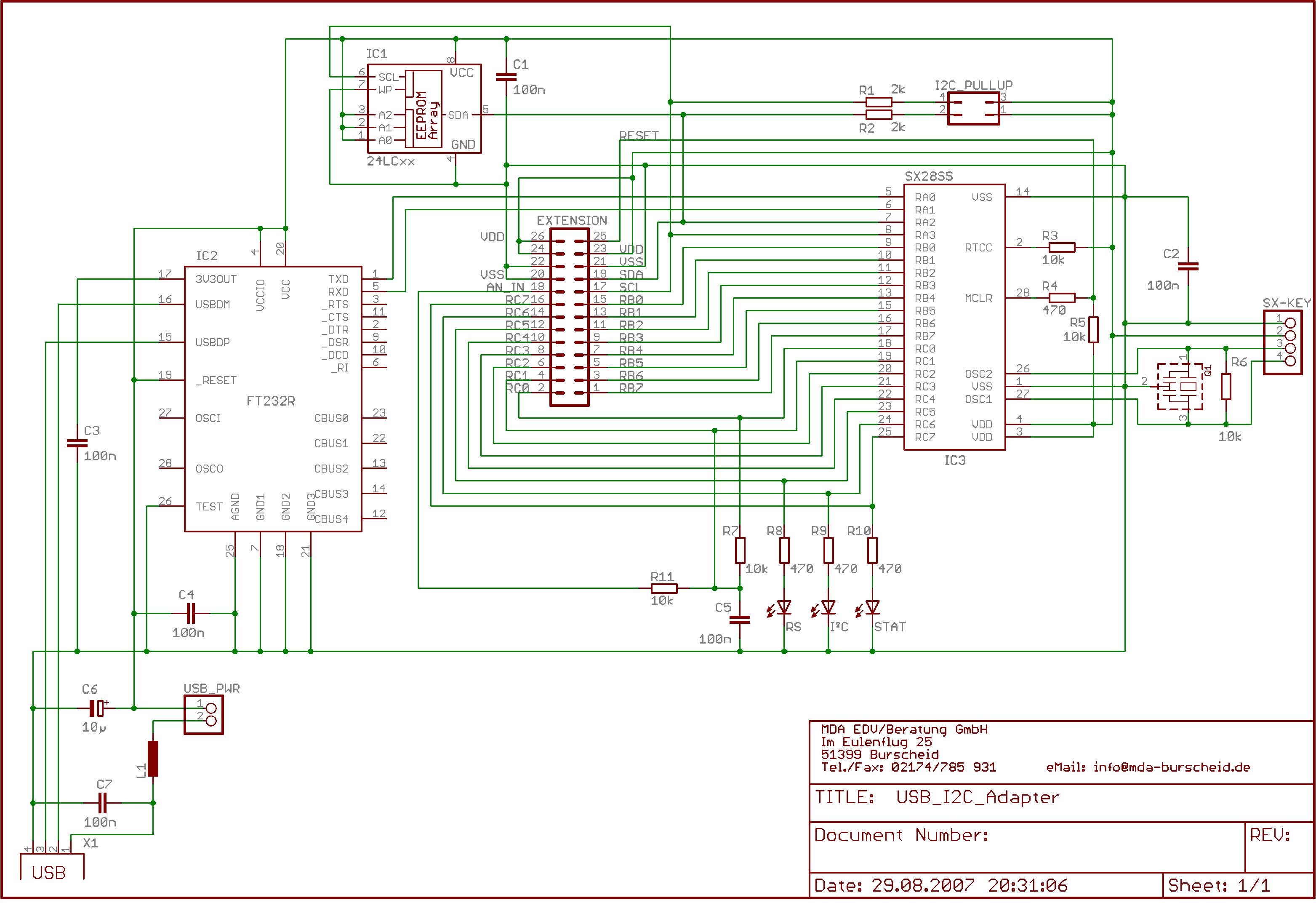
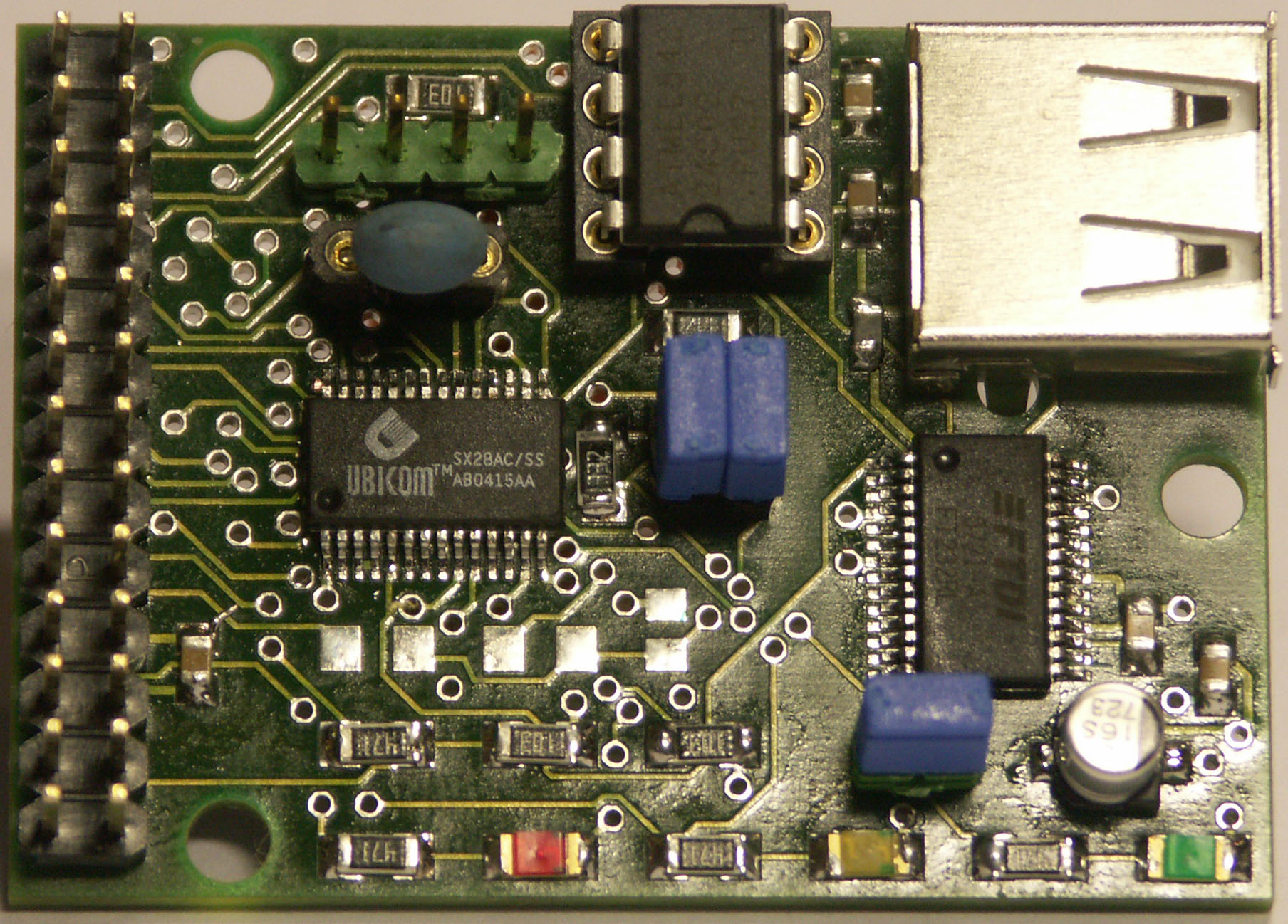
See the attached picture, and the schematic for the details. Besides the FT232R, and an SX28AC/SS, there is a socket for an optional serial EEPROM (24C??). Two jumpers are used to activate/deactivate the on-board I2C pull-up resistors, and another jumper optionally feeds-through the 5V from the USB port. So the board components can either powered from the USB port, or an external regulated power supply, connected to the Vdd/Vss pins of the 26-pin header. On this header are also available all SX28 port pins, the /MCLR pin, and an analog input/output for a bitstream ADC or PWM-controlled DAC. There are also pads for the ADC/DAC components (not installed on the board shown in the picture). Three status LEDs can also be installed, as well as a resonator, and the famous SX-Key 4-pin header.
I have hand-soldered all components on the sample board shown in the pucture, including the FT232R, and the SX28AC/SS. For both, I used the "solder all, and clean with solder wick" technique, and it worked pretty well for me (after several beers to keep my hands calm ).
).
Like the SX28 Multi Board, this is a 4-layer board with two inner supply layers. The layer closer to the top is connected to Vss, and the layer closer to the bottom to Vdd, and on the bottom side (not shown here) there are large ground planes connected to Vss. So, the inner layers together with the bottom ground planes make an almost perfect filter cap that helps reducing EMI.
The board size is 50 by 35 mm.
BTW: The current version has a design flaw. It actually does not limit the operations of the board by any means, but it is a bit out of the rules. I don't tell you more about it - mayby you can find it out. The first forum member with the right answer will get one fully assembled board for free.
▔▔▔▔▔▔▔▔▔▔▔▔▔▔▔▔▔▔▔▔▔▔▔▔
Greetings from Germany,
Günther
a long time ago, I have presented here my SX28 Multi Board, designed for all plated-through components. In the meantime, I have used this board for many different purposes, like experimental projects, small series, and as base for my RS-232/I²C adapter/monitor. This board comes with a MAX232 to interface to a serial RS-232 port.
In the meantime, many new PCs no longer come with an RS-232 port, so I though it would be time to design a new board with USB interface. As all USB interface chips available (like the FTDI232R I'm using) only come in SMT packages, I decided to make use of SMT components all over the board (with a few exceptions).
See the attached picture, and the schematic for the details. Besides the FT232R, and an SX28AC/SS, there is a socket for an optional serial EEPROM (24C??). Two jumpers are used to activate/deactivate the on-board I2C pull-up resistors, and another jumper optionally feeds-through the 5V from the USB port. So the board components can either powered from the USB port, or an external regulated power supply, connected to the Vdd/Vss pins of the 26-pin header. On this header are also available all SX28 port pins, the /MCLR pin, and an analog input/output for a bitstream ADC or PWM-controlled DAC. There are also pads for the ADC/DAC components (not installed on the board shown in the picture). Three status LEDs can also be installed, as well as a resonator, and the famous SX-Key 4-pin header.
I have hand-soldered all components on the sample board shown in the pucture, including the FT232R, and the SX28AC/SS. For both, I used the "solder all, and clean with solder wick" technique, and it worked pretty well for me (after several beers to keep my hands calm
 ).
).Like the SX28 Multi Board, this is a 4-layer board with two inner supply layers. The layer closer to the top is connected to Vss, and the layer closer to the bottom to Vdd, and on the bottom side (not shown here) there are large ground planes connected to Vss. So, the inner layers together with the bottom ground planes make an almost perfect filter cap that helps reducing EMI.
The board size is 50 by 35 mm.
BTW: The current version has a design flaw. It actually does not limit the operations of the board by any means, but it is a bit out of the rules. I don't tell you more about it - mayby you can find it out. The first forum member with the right answer will get one fully assembled board for free.
▔▔▔▔▔▔▔▔▔▔▔▔▔▔▔▔▔▔▔▔▔▔▔▔
Greetings from Germany,
Günther


Comments
Taking a stab at your offer, is it that the components are installed on the solder mask side, instead of a silk screen side?
I like contests like this!
Thanks!
Rodney
I think it is capacitor C2 which is connected from VSS to VSS in the schematic.
Should be VSS to VDD.
rgeards peter
After taking a look I have found something that could be it. You have AN_IN tied to RC0 and RC1, assuming you meant this to be Analog input, it would be completely useless since there is no comparator, and the SXs comparator is on RB0-RB2. I cannot tell the reason the two resistors and the cap are there other than a filter for analog input, that was accidentally placed on the wrong I/O bank.
-Kris
I'll have to guess that pin 1 on the 8 pin socket should have been pointing up. For esthetic reasons only.
Rodney: Actually, the bord has solder mask prints on both sides, and no silk screen for now, so the components are located on the correct side. Sorry, no hit
Peter: Wow, you really found a bug, that I did not recognize so far, but this is not the flaw I was asking for, so the contest is still open. Anyhow, you have earned the merits for finding another bug which is worth an extra price, so one of the boards is yours!
Kris: The components R11, R7, and C5 are planned to be used for the popular "Continuous Calibrating Bitstream" Analog/Digital Converter virtual peripheral with RC.1 acting as sense input, and RC.0 as charge/discharge output, so the comparator at RB.0...RB.2 is not required for this purpose. RC.0 can also be used to output a PWM signal with R7/C5 acting as low-pass filter for digital/analog conversion. Sorry, no hit.
CCraig: Hmm - yes - I could rotate the 8-pin socket for the EEPROM by 180° without increasing the length of the copper traces but as you mentioned: This is an estetic matter only - no design flaw - sorry.
So, the contest is still open - keep going...
▔▔▔▔▔▔▔▔▔▔▔▔▔▔▔▔▔▔▔▔▔▔▔▔
Greetings from Germany,
Günther
I will PM you·my address.
I will not post another guess (even if I find it)
to allow others to win a board.
regards peter
I think I would have pulled the EEPROM address lines down instead of up.
Cheers,
Peter (pjv)
I can't really see it very well, but it looks like you have a USB-A connector. The FTDI is meant to be a slave correct? meaning that the USB gets connected to a computer and a virtual serial port is created. This would mean that in order to connect the board to a PC, a USB-A male to USB-A male cable is needed, which is hard to come by. There should be a USB-B jack (the square-ish one) on the board to making it easier to find cables to use.
-Kris
EDIT: Got my USB-B and USB-A mixed up, had to fix it
Post Edited (bunni) : 10/11/2007 12:38:33 AM GMT
Kris:
CONGRATULATIONS - you nailed it!
Yes, by mistake I used a USB-A connector for a slave device which usually should come with the "square-ish" one as you have mentioned it. Maybe, I was mislead by the INTRONIX logic analyzer I have here which also comes with the USB-A connector. Fortunately, I found a good supply for USB-A male to USB-A male cables.
Please PM me your mailing address, and I'll send you the board (plus the cable)
▔▔▔▔▔▔▔▔▔▔▔▔▔▔▔▔▔▔▔▔▔▔▔▔
Greetings from Germany,
Günther
The "official" contest is over now. Nevertheless - if you find more flaws, please feel free to report them. For major flaws reported, I'm willing to give away more boards for free (including the cable and the flaws
▔▔▔▔▔▔▔▔▔▔▔▔▔▔▔▔▔▔▔▔▔▔▔▔
Greetings from Germany,
G
No major design flaw, but you may consider placing small series resistors (270 ohm)
at pins RA0 (connects to TX), RA2 (sda) and RA3 (scl) to prevent these
pins to be damaged if they become outputs (RA0) or driven high (sda).
When scl is driven high on a multimaster bus that pin could also be damaged.
I assume you deliver some code routines to deal with onboard connections
but just in case of programming errors, it is better to know your board is
protected. The same protection rules of course also apply to external circuitry.
Another small protection would be a diode on the usb power line, just in case
the board is powered via the header and the usb jumper is in place.
It is very easy to forget about that jumper when plugging in a usb cable.
regards peter
thank you for your valuable hints. I agree with you, small resistors in series with the I/O pins are always a good idea for enhanced protection, especially on a multi-purpose board like this. I also like your idea concerning the protection diode in series with the USB power line. The only problem is the voltage drop across the diode, so the supply voltage would go down to about 4.4 Volt (provided that the USB voltage is not already below 5V which can be the case on "weak" systems). For the SX28 and the other components, the reduced supply voltage would not be a problem but an SX-Key/Blitz might not work correctly in this case.
One general remark to I²C: According to the specifications, no component on the bus is allowed to drive SDA or SCL high. It is only allowed to pull the bus lines low, or release them, so that they are pulled up to high level throught the resistors. On the other hand, when there is only one master in the system, it is ok to break this rule for the SDA line, provided that none of the slaves attached can initiate clock stretching (which the master also would have to support).
I'll collect all these good hints for the next board re-design.
Thanks a lot.
▔▔▔▔▔▔▔▔▔▔▔▔▔▔▔▔▔▔▔▔▔▔▔▔
Greetings from Germany,
Günther
You are right about I2C. Pins should be inputs or low outputs. But due to
programming errors (wrong page bits etc.) the pins could become
high outputs accidently.
I didn't consider the sxkey when mentioning the diode. May be
interesting to test if the sxkey functions properly with 4.3 volts.
Or use a germanium diode which only has 0.3V drop.
regards peter
Another option is to use a 3pin header for the jumper to either
apply usb power or external power to the board.
That way there never can be a conflict and no diode
is required.
regards peter
And yes, it is supposed to be hooked up backwards [noparse]:D[/noparse]
Here is a good picture
http://electronicdesign.com/Files/29/9945/Figure_01.gif
and explanation
http://electronicdesign.com/Articles/Index.cfm?AD=1&ArticleID=9945
regards peter