

Can someone compare my working BS2 program to my non working SX28 program? (Use
 T&E Engineer
Posts: 1,396
T&E Engineer
Posts: 1,396
I have a working BS2 program that interfaces to a 8255 chip for 24 outputs. I tried to port this to the SX28 and did not get anything displayed (LED's test).
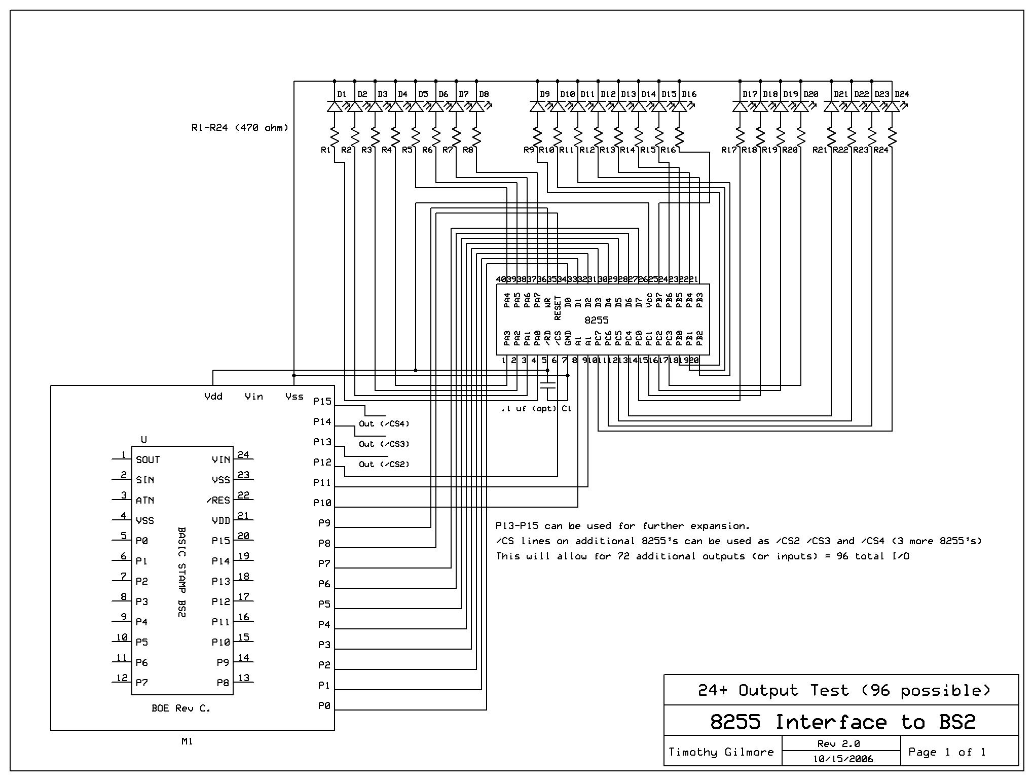
Here is the original post for the working BS2 to 8255 circuit:
http://forums.parallax.com/showthread.php?p=561893
The main differences in the drawing between them are:
SX-28 chip used instead of BS2px (also works with BS2)
Control pins (Reset, WR, A1, A0 and CS) are on RB (I could not get them to work on RA and RB.0 either)
There doesn't seem to be an OUTS and DIRS for SX/B so I·tried RB·= $FF and $00···to represent HIGH and LOWs· (and TRIS_RB, etc..) to·make it match the BS2 code closer. Using standard HIGH and LOW statements didn't cut it either. Nothing worked again so I used the new PIN statement (hard to find any info on how to use this - Where's the HELP file?)
I then suspected it might be the PAUSE and PULSOUT commands·being timed·differently from PBASIC and SX/B.
I changed a little bit of the code to make it almost a 1 for 1 match with the BS2 code....·but it has not made any difference.
Could it be a timing issue - SX28 is too fast? I'm ready to listen as this doesn't make sense to me.
I can have both circuits (2 8255's) side by side and can swap them·between each circuit - using a Professional Development Board (PDB). I can read when there is a HIGH and LOW· on the 8255 pincs using a multimeter to an extent - but still uncertain about the PULSOUT if that operates differently. I have also put in a known good working SX28 chip too.
I simply don't see what may be happening here and what I want to know is if there is any significant changes betwen PBASIC and SX/B that would cause no LED outputs from the SX28 8255 circuit.
I very much appreciate any input to this problem.
Thanks again!
Post Edited (T&E Engineer) : 10/21/2006 10:16:27 PM GMT

Comments
It appears that the SX-28 is sending all of the right programing out of it's RB / RC outputs (as various parts of the code were issolated to test).
This leaves one variable left that I can think of. Is the SX-28 too fast for the 8255? I tried changing the DEVICE and FREQ statements for an internal 32KHz and·the·SX28/8255 circuit·still did not function. Correct signals appear to be coming out of the SX28 as far as I can tell.
I can take this same 8255 out of the SX28 circuit and put it in to my working BS2px circuit and it functions correctly.
As you can see the SX-28 code has been modified for almost a 1 to 1 coding correspondance between the BS2px code and the SX-28 code.
Please help if you can as this is driving me a bit crazy tonight.
Thanks.
On the BS2 / 8255 working circuit I saw either ~4.9 v or ~0 v.· However, on the Sx-28 / 8255 non working circuit I saw ~2.8 v on the CS pin and ~3 v on the WR pin and the other pins were ~0 v.
Does this mean that the SX-28 can not drive the BS2 and needs to be buffered? That would certainly explain why it is not working.
I have·some buffer chips and I will try this if anyone agrees.
Comments?
Thanks.
If so then you should have pins set low for both high and low signals and toggle the port direction from input (high signal) to output.low for the low signal. The basic stamp code uses HIGH CS_8255 where normally you would switch the output low on the CS to input highz to allow the pullups to pull the line high.
Like I said Its 2:30 and I am just trying to get out of here but I thought i would toss that out there.
Gnight..
▔▔▔▔▔▔▔▔▔▔▔▔▔▔▔▔▔▔▔▔▔▔▔▔
Think outside the BOX!
I have a program written for a Parallax Basic Stamp 2 (BS2) microcontroller and 8255 Interface circuit that works with 4.9v on CS and WR control lines and ~0v on A1, A0 and RESET control lines.
I wrote a almost 1-1 identical program for Parallax SX-28 microcontroller. However, as originally written, I get 2.2v on CS and 3v on WR control lines and ~0v on A1, A0 and RESET control lines. I can even pull all of these control line wires between the SX-28 to the 8255 and take measurements directly from the SX-28 and get those same 2.2v and 3v measurements.
I tried adding a 74HC245 buffer (/OE tied to ground and DIR tied to +5v) on CS and WR control lines between the SX-28 and 8255 and saw no differences in the voltages readings (2.2v and 3v). I removed it.
I tried adding some pull up 10K resistors from +5v to the CS and WR lines and saw no changes in voltage (actually a bit of a drop) and no circuit working still for the SX-28 and 8255. I also tried resistors from ground to the CS and WR lines and it did not work either. I removed the resistors.
What is different between the BS2 and SX-28 to cause different voltage differences of 2.2v and 3v when the BS2 generates 4.9v on both control lines?
I have run out of ideas on this one. Please help (anyone).
Thanks.
Post Edited (T&E Engineer) : 10/22/2006 2:13:58 PM GMT
Although I have not looked at your code (my SX/B skills are minimal), I would suggest that your SX/B software operates differently from what you think it is doing, and the lines in question are actually pulsing for some (software) reason.
Can you look at it with a scope?
Cjeers,
Peter (pjv)
▔▔▔▔▔▔▔▔▔▔▔▔▔▔▔▔▔▔▔▔▔▔▔▔
Think outside the BOX!
Both BS2 and SX/B programs are almost identical but the voltages are correct ~5v coming out of the WR and CS control lines of the BS2 circuit and incorrect at 3v and 2.2v (not 5v) coming out of the same control lines on the SX-28 circuit. There is something differently happening in the SX-28 that needs to be explained.
I don't have a scope·just a multimeter.
oops nevermind thats just for intpt threshold
I guess the scope shows a ful 5V on the pins on my SX28.
What do you get with no load on the pin, do a program to set the pin high and measure it
By the way as you can see in the scope you have about a 50% duty cycle on those two pins so you would not measure 5V with a slow meter while your program is running.
Hey I will do the same test with the scope on the BS2, be back in a few...
Hey maby thats it, I did it on the BS2 not BS2px but the CS is held low for way longer than the sx, so perhaps you need to pulsout a longer WR and hold the CS low longer. Actually I think you need to pause after you set the CS low before you pulsout the WR as the transition is what is being missed by the 8255.
▔▔▔▔▔▔▔▔▔▔▔▔▔▔▔▔▔▔▔▔▔▔▔▔
Think outside the BOX!
Post Edited (metron9) : 10/22/2006 10:34:07 PM GMT
With no program running on either the BS2 or SX-28, I get send HIGH statements to send out +5v so this is not an issue.
The issue is when running my program on the SX-28, it gives my CS pin 2.2v and my WR pin 3v with no load on the pins.
On my BS2 runing an almost identical program it gives 5v on both CS and WR as it should and it does run correctly.
Are you running my SX-28 program? If so you can see what I mean. The same goes for my BS2 program.
I tried what you said but it only brought CS down to 0v.
However, I put in a PAUSE 50 (had to be higher than PAUSE 10 to get a good voltage over 4.9v on CS) after the HIGH CS1_8255 and before the RETURN statements and got rid of all of the other PAUSE statements that was in trial and error.
Now I get the same voltages out (~4.9v on WR and CS) as the BS2 gets ( and ~0v on the others) but still does·NOT work on the SX28.
I also tried swapping the 8255's and the problem is only on the SX28 circuit no mater what 8255 is used. The BS2 program always works but the SX28 never does even now with the same control voltages coming out of the SX28 to the 8255.
HELP!!
Just for fun, try using a pause 1 between every high and low code in both the initialize code and the subroutines. It may be at high speeds the transitions are not doing what you think they are because of stray capacitance or something else. If it's not that then all I can offer is more scope output on pins you wish to see using the sx28 chip.
▔▔▔▔▔▔▔▔▔▔▔▔▔▔▔▔▔▔▔▔▔▔▔▔
Think outside the BOX!
I need some help perhaps by Parallax or Bean maybe to see what is so different in the timing between the SX-28 and the BS2. I have tried everything under the sun and the SX-28 program still shows no output LED's unlike the BS2 version which is running fine with no extra PAUSE statements needed.
Perhaps since it is the work week now, I can get some more help with a different perspective.
THIS SX-28 PROGRAM (ABOVE) DOES NOT WORK
THIS BS2 PROGRAM (BELOW) DOES WORK ---- WHAT IS DIFFERENT BETWEEN THEM?
' {$STAMP BS2px} ' {$PBASIC 2.5} ' ' 8255 PPI IC - Test program with 24 outputs available. ' Written by Timothy Gilmore ' 10/15/06 ' ' Test program using the 8255 and BS2PX (OR BS2). ' ' ----- Constants Reset_8255 PIN 8 WR_8255 PIN 9 A0_8255 PIN 10 A1_8255 PIN 11 CS_8255 PIN 12 ' 3 additional 8255 chips can be used when using: ' CS2_8255 PIN 13 ' CS3_8255 PIN 14 ' CS4_8255 PIN 15 ' This would provide 24+24+24 additional inputs and/or outputs (96 I/O lines possible) ' Modify the code below to add the 3 additional Chip Select lines if needed to add more 8255's. ' ----- Variables pattern1 VAR Byte pattern2 VAR Byte pattern3 VAR Byte ' ----- EEPROM Data ' ----- Initialization OUTS = $00 ' Set Outputs Low DIRS = $FF ' Set I/O Direction GOSUB Initialize_8255 ' ----- Main Code Main: pattern1 = %10101010 'Set pattern for Output Ports (Read it in reverse) pattern2 = %11110000 pattern3 = %00110011 GOSUB PortA_8255 GOSUB PortB_8255 GOSUB PortC_8255 GOTO Main ' ----- Subroutines Initialize_8255: 'Initialize 8255 to All Outputs at Active Low state OUTH = $FF 'Set all the control lines (P8-P15) High (Inactive) PAUSE 50 'Settling time for a few ms (50 ms) LOW Reset_8255 '8255 is Reset (Active) HIGH WR_8255 'Set Write control High (Inactive) HIGH A1_8255 'Set Address control A1 & A0 High to access the control word register HIGH A0_8255 OUTL = $80 'Set databus (P0-P7) to $80 for MODE 0 - All 3 ports as outputs LOW CS_8255 'Set Chip Select Low (Active) PULSOUT WR_8255, 50 'Pulse Write control Low (Active) for 100 us (duration not critical) HIGH CS_8255 'Set Chip Select High (Inactive) - All outputs are set to Active Low RETURN PortA_8255: 'Set up 8255 Port A for Output LOW A1_8255 'Set address control A1 & A0 Low to set the 8255 Port A for Output LOW A0_8255 OUTL = pattern1 'Set databus for pattern1 LOW CS_8255 'Set Chip Select Low (Active) PULSOUT WR_8255, 5 'Pulse Write control Low (Active) for 10 us (port changes state) HIGH CS_8255 'Set Chip Select High (Inactive) - Disable the 8255 databus RETURN PortB_8255: 'Set up 8255 Port B for Output HIGH A1_8255 'Set address control A1 & A0 to set the 8255 Port B for Output LOW A0_8255 OUTL = pattern2 'Set databus for pattern2 LOW CS_8255 'Set Chip Select Low (Active) PULSOUT WR_8255, 5 'Pulse Write control Low (Active) for 10 us (port changes state) HIGH CS_8255 'Set Chip Select High (Inactive) - Disable the 8255 databus RETURN PortC_8255: 'Set up 8255 Port C for Output LOW A1_8255 'Set address control A1 & A0 to set the 8255 Port C for Output HIGH A0_8255 OUTL = pattern3 'Set databus for pattern3 LOW CS_8255 'Set Chip Select Low (Active) PULSOUT WR_8255, 5 'Pulse Write control Low (Active) for 10 us (port changes state) HIGH CS_8255 'Set Chip Select High (Inactive) - Disable the 8255 databus RETURNI am sending·Metron9 a couple of 8255's this weekend that he can look at with his BS2 and SX-28 chips to replicate what I am seeing. He has a scope so he can see some timing differences. I can't believe that this is this difficult to figure out. I am lost for ideas. I did receive an old 1977 book today in the mail from Ebay called "Microcomputer Interfacing with the 8255 PPI chip" but it looks really out dated. Hopefully I can get some insight on this chip.
Although, I think the 8255 chip is ok but the SX-28 has timing issues with this chip.
Comments? Although I feel sometimes like no one is home.
It would not surprise me that the reason you are seeing a void in responses is your previous refusal to heed the advice given. What's the point of us spending our time when you scoff at the suggestions.
Please recall my and others' frustration with your LED project at the end of January of this year; to refresh your memory, refer to the link
http://forums.parallax.com/forums/default.aspx?f=5&m=103896
As is often the case, you reap what you sow, and I'm not prepared to put in a bunch of time with no appreciation for the effort.
I hope you can devise a means to break your problem into smaller and smaller pices so eventually you find the solution. And when you do, I expect it will be related to my comments·8 posts back.
Cheers,
Peter (pjv)
You're sounding like a spoiled newbie...
It's going to very difficult to troubleshoot timing problem without an oscope.
Try anything and everything you can think of. It's probably something simple.
Bean.
▔▔▔▔▔▔▔▔▔▔▔▔▔▔▔▔▔▔▔▔▔▔▔▔
Cheap used 4-digit LED display with driver IC·www.hc4led.com
Low power SD Data Logger www.sddatalogger.com
SX-Video Display Modules www.sxvm.com
"People who are willing to trade their freedom for·security deserve neither and will lose both." Benjamin Franklin
Post Edited (Bean (Hitt Consulting)) : 10/25/2006 1:16:45 AM GMT
I just don't understand·why it works on a BS2·but get nothing on a SX-28.
I·am having an expert in the ZX81 community Wilf Wrighter help me with this on a ZX81 forum as he is one of the pioneering people that has many years experience with the 8255. He has been a great help for me to try things in the code. However, it seems to be apparent the issue is with the SX-28. You're right about needing a scope and Metron9 has been gracious enough to help me troubleshoot this.
I have not gotten much sleep working on this at night and I appologize if I have affended anyone.
Thanks for the good advice Bean.
I looked at the datasheet and noticed that the minimum timings and they are all in the ns range which is pretty small so technically your previous timings should be ok.
Look at the datasheet ( http://www.intersil.com/data/fn/fn2969.pdf·) for timing information.· Also, make sure you pull the RD line high for basic output mode 0.
Harrison
I tried inserting PAUSE 10 all the way to PAUSE 1000 between every statement in the Initialization_8255 and PortA routines. I have also increase the PULSOUT WR_8255, 10 to various high and low ranges. I have checked and rechecked the 5 control line wires over and over and they are correct as the PIN statements have stated. I have changed values of RB and RC from $00 to $FF and $FF to $00 many times over now to look for changes. I always turn up with no output on the LEDs. I know he 8255 works as I have a BS2 connected to another 8255 runing an almost identical program (with no PAUSE statements like the SX-28 has) and it runs great producing the pattern statement code on the LED outputs. I can swap the 8255's between the BS2 and SX-28 circuits and the SX-28 circuit never produces any LED outputs. However, the SX-28 8255 (when swapped over to the BS2 circuit) works fine. So I know the 8255 circuit works. I can also connect a multimeter to the SX-28 pins and produce various HIGH and LOW statements on all the RA, RB and RC pins to test to make sure they work and they do. However, with no PAUSE statements inserted into the SX-28 code, the WR_8255 and CS_8255 pins on the SX-28 (RB.1 and RB.4) do not produce ~5v out on them like they do on their BS2 circuit equivalent. With additional PAUSE statements added to the SX-28 coding, I do get ~5v as they appear the same on the BS2 circuit equivalent. This tells me that the timing is different in the SX-28 than the BS2 which make sense somewhat because the SX-28 runs much faster than the BS2. However, I can also get the same BS2 circuit to run the same on a BS2px (3 times faster than a standard BS2).
I have changed so many items in the SX-28 code, I don't really know what to look at next. It does sound like a timing issue and Metron9 will be sent 2 8255's to recreate what I am seeing here on my BS2 and SX-28. He has a scope to look at timing issues so maybe we will learn something a week from now. However, in the mean time I reach out to the Parallax community to see if they have any sugestions to try since it clearly seems to indicate a problem with the SX-28 coding and not the 8255.
Thanks again!
Have you tried swapping the 8255 from the working circuit with the 8255 in the non-working circuit? The 8255 came in various timing flavors as well as NMOS and CMOS versions. Years ago I had a circuit that would only work with the CMOS version. Rather than spend time figuring it out, I simply bought CMOS chips and everything worked fine. Are the 8255 chips you're using identical in every way?
Thanks,
PeterM
I stated earlier that I am able to swap many different 8255's from various manufacturers (I have 13 of them) and they pretty much work on the 8255 circuit for the 4-5 of them I have tried but do not on the SX-28 circuit.
Thanks for checking.
PS: How do I tell if I have the CMOS version? I may not have this if it is listed as 82C55A. C is for CMOS? God I hope I don't have to buy more of them. Lol. I have the standard ones I think from Intel, NEC (e.g. 8255A) but I will look again. I am going out of town on business and won't be able to check on this till Friday but I will let you know although I don't believe I have an CMOS version. Static Sensitive. Yikes.
Bad news first:
The chips were not in the plastic case, good thing you used bubble envelope they are ok, I fixed the bent pins.
I tested it on a BS2, runs fine
I tested it on the SX and had very odd starts and stops, sometimes it worked sometimes it did not work.
From my experience that can mean two things. Power to the chip, or loose connections. I checked the power, the chip is only drawing 24mA and the power from the SX board is fine.
The good news:
Loose connections, that was my problem, the pin headers on my SX totally suck, RB4 I had to use an extra thick wire to even make a connection. When I got all the connections tight, I cranked her up to 50MHZ. No problem with the original code, I removed all pause commands and dropped the WR pulsout in the subs to 1 instead of 10. No problem at 50MHZ
You have loose connections or you have some wires crossed. I also did not use the .1 cap
I ran a test at 50mhz sending to portC with no delay the first loop (too fast to see) then with 1mS delay alternating between loop 1 and loop 2. No glitches runs perfect.
Let me know what you find.
Test Code: turns on 8 led's in sequence from nit 0 to bit 7 on PORT C
▔▔▔▔▔▔▔▔▔▔▔▔▔▔▔▔▔▔▔▔▔▔▔▔
Think outside the BOX!
I also did not use any external resonators. I used by my orginal code 4 MHz internal to the SX-28. Can you post the exact code and hardware connections you made. Did you use a PDB or wire up the SX-28 on a solderless breadboard, etc..? I don't want to leave anything to guess work this time.
Comments?
Post Edited (T&E Engineer) : 11/2/2006 11:09:02 AM GMT
▔▔▔▔▔▔▔▔▔▔▔▔▔▔▔▔▔▔▔▔▔▔▔▔
Think outside the BOX!
I tried your code and {my code (attached)} on the Parallax Professional Development Board and got nothing. I then used a separate solderless breadboard (not on the PDB) and only wired +5v and GND from the PDB to it as well as ran 2 wires from the PDB Y1 jack to the separate solderless breadboard for OSC1 and OSC2 signals. Remember all I have going from the PDB to the separate solderlessbreadboard·(similar in·your setup)·is +5v, GND, OSC1 and OSC2.
On the separate solderless breadboard, I wired up a SX-28, 8255 and 8 LEDs/resistors. The 4 lines of +5v, GND, OSC1 and OSC2 were connected from the PDB.
I only connected the 8 LEDs/resistors to PA0-PA7. Of course I connected the D0-D7 8255 lines to RC.0 - RC.7 and 5 control lines (RESET, /WR, A0, A1, /CS) to the SX-28 (RB.0 - RB.4). On the 8255 (+5v on pins 26, 5) (GND on pin 7). On the SX-28 (+5v on pin 2) (GND on pin 4). The SX-28 had a 10K resistor from +5v to pin 28 (/MCLR) as it shows in the PDB schematic. The OSC1 and OSC2 PDB lines were run into pins 27 and 26 (SX-28) respectively. The +5v and GND lines were run from the PDB to the separate solderless breadboard.
At this point everything is setup correctly to at least look at the 8255 Port A.
SUMMARY:
Your "SXBtest.sxb" program gave me no outputs on the LEDs when programmed on either the PDB SX-28 or the separate solderless breadboard SX-28 circuit.
However, I did run my code (attached) and IT DID WORK as expected.
WHAT DOES THIS MEAN?
It first tells me that something on the Parallax Professional Development Board is not making contact. Normally I seem to have no problems programming it on the PDB (or separate solderless breadboard) and can even send HIGH and LOWs to the on board LEDs/resistors.
I will try replacing part by part back onto the PDB and try to get my code working again. Once I find out what the culprit problem is with the PDB, I may need to call Parallax up to see if anything can be done.
Once this is resolved and get "something" working on a combinational effort between the PDB and the separate solderless breadboard, I will see what the differences are between Metron's SXBtest code and mine.
I have never seen this much trouble in my life in troubleshooting irregularities on 2 different setups.
It has certainly been a lesson learning experience in my life.
Comments????
Thanks for putting up with my persistance to solve this strangeness.
Yikes sorry, I changed the code to only call port C mot A, that's why it's not running, it was eaiser to wire those pins that's why.
▔▔▔▔▔▔▔▔▔▔▔▔▔▔▔▔▔▔▔▔▔▔▔▔
Think outside the BOX!
Post Edited (metron9) : 11/3/2006 5:30:24 PM GMT
Keep in mind that the info below only refers to the second circuit built on a separate solderless breadboard as described earlier. I have not troubleshooted my PDB yet. More to come on this.
However, I went through your code and changed the lines of PortC_8255 to PortA_8255 and it worked. I should have hooked up all of the LEDs for your program.
What else was odd was that I removed every occurance of PAUSE statements in my program (attached) and IT STILL WORKED so timing was not an issue (conditions of 4 MHz and 50 MHz)
But I also noticed that I can use your 50 MHz Device lines and it does work (sort of) in yours and my program. What I did notice is that when I use the 50 MHz settings and turn power off and on quickly a few times it does not always turn the LED's on. It's like it misses the timing and it stays off.
BUT...if the device lines are set to 4 MHz, I have no problem with either program when power is switched on and off quickly a few times. All the correct LED's come on as they should from the program code.
All the wires I am using are about 1-3" long on average with the longest being maybe 6".
NOW: My guess is that as far as the PDB goes, it will most likely be an issue with the SX-28 socket. I will still have to test this and find out for sure. More to come.
Good work !!!!
Comments??
Post Edited (T&E Engineer) : 11/3/2006 7:12:01 PM GMT
This program cycles through (1/2 second each LED) all 24 outputs (3 * 8). It took me only a few minutes to convert it over from a BS2 version I had of it.
Comments??
Now it's time to troubleshoot the PDB...
More to come.
But even if it isnt the initialize code has no effect on the loop it would just leave the pins in an unknown state and the loop would run normal.
The HIGH A1_8255 is the SX initializes pin so unless it was set to low somewhere else that would not be the problem.
50mhz is pushing the limits of a breadboard though, depending on the type of breadboard and atmospheric conditions you could have too high capacitance that holds a line high for too long at high speeds, or creates noise similar to a pushbutton switch toggeling the line, without a scope you cant be sure what's going on in that time frame.
Glad it is working. Now i need a new harder problem to solve.
▔▔▔▔▔▔▔▔▔▔▔▔▔▔▔▔▔▔▔▔▔▔▔▔
Think outside the BOX!
Step 2. I moved the SX-28 back into it's socket on the PDB and left the 8255 wired to the separate solderless breadboard and it worked.
Step 3. I moved the 8255 onto the PDB (with the SX-28 in it's normal socket) and IT WORKED.
HOW IS THIS POSSIBLE????
I originally had it like this and why should it all of a sudden work now?
Perhaps the SX-28 needed to be reseated back into it's socket?
Perhaps the wires were getting bent arround too much?
It still blows my mind on why it works correctly in the PDB now....
I don't know if I buy any of this but what I do know is that both the BS2 and SX-28 circuits work on the PDB with any 8255 chip.
Case closed.
Wow this was a really hard one and very fustrating!!!!
Special thanks goes out to Metron9 who stuck by me and was able to go the extra mile to help!·· Great Job!!!
My next step is to get a second 8255 (e.g. 48 outputs) to work with the SX-28 and BS2. This should be a piece of cake since I can have multiple CSx_8255 (chip select lines). I will post my findings probably in a new Thread.
After this I will learn how to interface it to a ZX81 computer expansion port (which may or may not be of interest to this community). I have all of the right tools and equipment to make it happen.
Thanks again Metron9!
BTW: I did now measure 4.95v on the CS and WR lines (as this was at 2.2v and 3v previously I beleive {but could still be brought up to ~5v with additional PAUSE statements - of which now I have NO PAUSE statements in this final software version}. WEIRD!
Post Edited (T&E Engineer) : 11/3/2006 8:40:44 PM GMT
For more on Read/Modify/Write problems (which are a seperate issue) see:
http://www.sxlist.com/techref/readmodwrite.htm
This is really good information to know thanks James.
It looks like that could very well be the problem in this code!
Perhaps use pause between setting HIGH's or write the whole port at once.
Initialize_8255: 'Initialize 8255 to All Outputs at Active Low state
RB_OUT = $FF 'RB pins (Control lines are set Inactive HIGH)
' PAUSE 1 'Settling time for a few ms (50 ms)
LOW Reset_8255 '8255 is Reset (Active)
HIGH WR_8255 'Set Write control High (Inactive)
HIGH A1_8255 'Set Address control A1 & A0 High to access the control word register
HIGH A0_8255
RC_OUT = $80 'Set databus (D0-D1 of 8255) to $80 for MODE 0 - All 3 8255 ports as outputs
LOW CS1_8255 'Set Chip Select Low (Active)
PULSOUT WR_8255, 10 'Pulse Write control Low (Active) for 100 us (duration not critical)
HIGH CS1_8255 'Set Chip Select High (Inactive) - All 8255 outputs are set to Active Low
RETURN
Think outside the BOX!
Back to Top
▔▔▔▔▔▔▔▔▔▔▔▔▔▔▔▔▔▔▔▔▔▔▔▔
Think outside the BOX!
▔▔▔▔▔▔▔▔▔▔▔▔▔▔▔▔▔▔▔▔▔▔▔▔
Chris Savage
Parallax Tech Support