

BS2 and MAX1270 help please
 Dru
Posts: 10
Dru
Posts: 10
Hello, I have a BS2 board setup with a MAX 1270 ADC. The project is to monitor an engine in a car for efficiency purposes.
These are my goals:
Sample 0-5+ V in all 8 channels.
Use internal clock of MAX 1270, for 1 sample per second of each 8 channels. (8 diff samples per sec)
So forgive me if I am asking simple questions.· I cannot seem to get things going in any way.
I've used a schematic and code I found on the web:
Except for I do not have the reference adjust hooked up; don't have those capacitors.
I have a POT supplying 0-5 V for testing purposes. I'm using the following CODE. Note, the code syntax is for a BS2SX, but I have a· BS2.· But it runs.
My output is 0· DECIMAL for both portions of the outputbyte.. one for the first 8 bits, and another for the 4 remaining bits. (12 bit sample)
CODE::::· THANK YOU FOR YOUR TIME! - DRU
'{$STAMP BS2}
''
'' Programmer:···· Craig Stuart Sapp <craig@ccrma.stanford.edu>
'' Programmer:···· Florian Vogt <fvogt@ccrma.stanford.edu>
'' Creation Date:· Sat 10-23-1999
'' Last Modified:· Sat 10-23-1999
'' Filename:······ max1270.bsx
'' Syntax:········ Basic Stamp IIsx
''
'' Description:··· This program reads in samples from the
''················ Maxim 1270 (a 12-bit, 8 channels A/D chip).
''················ The sampled value is then printed on the computer screen.
''
clockpin··· CON···· 7··· ' synchronous clock pin to control MAXIM 1270 chip
inputpin··· CON···· 8··· ' for reading data from MAXIM 1270 chip
outputpin·· CON···· 9··· ' for sending the controlbyte to the MAX1270 chip
sleeptime·· CON·· 250··· ' time in milliseconds to wait between samples
msb········ CON···· 1··· ' mode for shiftout functions: msb
behindclock CON···· 2··· ' mode for shiftin: msb post clock
' the MAX1270 control byte below is composed of several fields
'· listed here from MSB to LSB bits:
'· bit7:···· defines the beginning of the control byte
'· bits4-6:· selects the A/D channel (0-7).
'· bit3:···· choose the A/D voltage range, 0=5v, 1=10v
'· bit2:···· choose polar/bipolar range, 0=positive, 1=positive/negative
'· bit0:···· choose clock mode: 0=internal, 1=external
'· bits0-1:· 10=standby, 11=power-down (clock mode unaffected)
'
' the control byte 1,000,00,01 means: channel 0, 0 to +5v, external clock:
controlbyte··· CON·· %10000001
' Variables:
bytea··· VAR···· Byte········ ' for holding first 8 MSBs of 12-bit sample
byteb··· VAR···· Byte········ ' for holding 4 LSBs of 12-bit sample
' According to BASIC Stamp Programming Manual v1.9, page 208:
' "Unused pins that are not connected to circuitry should be set to output"
' to minimize power consumption, which is done here:
DIRS = %1111111101111111
' Don't set pins connected to input circuitry to be output, or you can
' damage the Basic Stamp.
' Commands used below:
'
' SHIFTOUT···· outputpin, clockpin, mode, [noparse][[/noparse]data \ bits]
'·· outputpin = pin to send synchronous data on
'·· clockpin· = pin to send synchronous clock signal
'·· mode····· = 0=LSB, 1=MSB
'·· data····· = data to send
'·· bits····· = number of bits in data field to send (default = 8);
'
' SHIFTIN···· inputpin, clockpin, mode, [noparse][[/noparse]variable \ bits]
'·· inputin·· = pin to receive synchronous data on
'·· clockpin· = pin to send synchronous clock signal
'·· mode····· = 0=LSB, 1=MSB
'·· variable· = location to store the bits
'·· bits····· = number of bits to input (default = 8);
'
top:
·· ' first tell the MAX1270 that you want a sample from channel 0
·· SHIFTOUT··· outputpin, clockpin, msb, [noparse][[/noparse]controlbyte \ 8]
·· ' wait 4 clock cycles until the sample is ready to be returned
·· SHIFTOUT··· outputpin, clockpin, msb, [noparse][[/noparse]0 \ 4]
·· ' read in the returned sample from the MAX1270 chip
·· SHIFTIN···· inputpin, clockpin, behindclock, [noparse][[/noparse]bytea \ 8]
·· ' finish reading in the data (12-bit sample)
·· SHIFTIN···· inputpin, clockpin, behindclock, [noparse][[/noparse]byteb \ 4]
·· DEBUG DEC ? bytea
·· DEBUG DEC ? byteb
·· DEBUG CR
·· ' now wait a while before taking another sample
·· PAUSE······ sleeptime
····· DEBUG CLS
GOTO top:
Comments
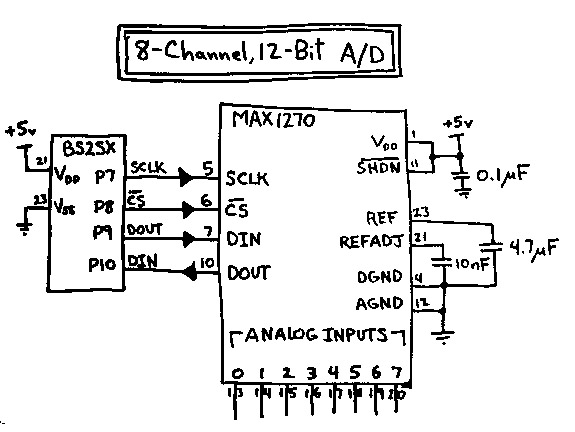
See the schematic. Pin 8 verses 10 on the BS2.
I get 255, 15 for positive voltage.. ie 111111111111. When the testing voltage is negative it turns to 0 again.
Is there code missing regarding BS2 pins 8 and 10?
Thank you. -Dru
heres my code
and heres my control bit... 0-10 vdc, no power down, internal reference is %10001000
the datasheet on the max1270 is one of the better ones i've found, have copied several of its charts into my code
good luck
'' max1270 ADC
'' -- dan miller
'' -- 16 july 2006
''
CON
· _clkmode····· = xtal1 + pll16x······················· ' use crystal x 16
· _xinfreq····· = 5_000_000
·
· ClkAdc······· = 5············ ' A/D clock
· CsAdc········ = 4············ ' Chip Select for ADC
· AoutAdc······ = 3············ ' A/D Data out
· AinAdc······· = 0············ ' A/D Data in
·
·
{{
Table 1. Control-Byte Format
BIT 7(MSB)·· BIT 6 BIT· 5 BIT 4 BIT 3 BIT 2 BIT 1· BIT 0(LSB)
START······· SEL2· SEL1·· SEL0· RNG·· BIP·· PD1··· PD0
BIT······· NAME·········· DESCRIPTION
7 (MSB)··· START········· First logic 1 after CS goes low defines the beginning of the control byte.
6········· SEL2·········· These 3 bits select the desired “on” channel (Table 2).
5········· SEL1
4········· SEL0
3········· RNG··········· Selects the full-scale input voltage range (Table 3).
2········· BIP··········· Selects the unipolar or bipolar conversion mode (Table 3).
1········· PD1··········· Select clock and power-down modes
0 (LSB)··· PD0
·Channel Selection
SEL2 SEL1 SEL0 CHANNEL
0··· 0··· 0··· CH0
0··· 0··· 1··· CH1
0··· 1··· 0··· CH2
0··· 1··· 1··· CH3
1··· 0··· 0··· CH4
1··· 0··· 1··· CH5
1··· 1··· 0··· CH6
1··· 1··· 1··· CH7
·Power-Down and Clock Selection
PD1·· PD0·· MODE
0···· 0···· Normal operation (always on), internal clock mode.
0···· 1···· Normal operation (always on), external clock mode.
1···· 0···· Standby power-down mode (STBYPD), clock mode unaffected.
1···· 1···· Full power-down mode (FULLPD), clock mode unaffected.
RANGE AND POLARITY SELECTION FOR THE MAX1270
INPUT RANGE···· RNG···· BIP···· Negative FULL SCALE···· ZERO SCALE (V)· FULL SCALE
0 to +5V·········· ·0······ 0······ —······················ 0·············· VREF x 1.2207
0 to +10V········ ·1······ 0······ —······················ 0·············· VREF x 2.4414
±5V················ ·0······ 1······ -VREF x 1.2207········· 0·············· VREF x 1.2207
±10V·············· ·1······ 1······ -VREF x 2.4414········· 0·············· VREF x 2.4414
for example 0-10 vdc, no power down, internal reference is %10001000
How to Start a Conversion
The MAX1270 uses either an external serial
clock or the internal clock to complete an acquisition
and perform a conversion. In both clock modes, the
external clock shifts data in and out. See Table 4 for
details on programming clock modes.
The falling edge of CS does not start a conversion on
the MAX1270; a control byte is required for
each conversion. Acquisition starts after the sixth bit is
programmed in the input control byte. Conversion
starts when the acquisition time, six clock cycles,
expires.
Keep CS low during successive conversions. If a startbit
is received after CS transitions from high to low, but
before the output bit 6 (D6) becomes available, the current
conversion will terminate and a new conversion will
begin.
}}
OBJ
· bs2·· : "bs2_functions"
·
· delay : "timing"
·
var·· long stack1[noparse][[/noparse]20]
·
pub start(control,average,ADC_addr)
· cognew(get_count(control,average,ADC_addr),@stack1)
·
·············
pub get_count(control_bit, average_sample, ADC_count_address) | temp, adresult_temp
·· repeat
····· adResult_temp := 0
····· repeat average_sample···························· '' how many samples to average
·······
······· delay.pause1ms(10)····························· ' wait 10 msecond···
······· outa[noparse][[/noparse]CsAdc] := 0······························· '' signal chip select
·····
······· bs2.SHIFTOUT(AoutAdc, ClkAdc,control_bit, BS2#MSBFIRST,8 ) '' put the control bit out
······· outa[noparse][[/noparse]CsAdc] := 1············································
······· outa[noparse][[/noparse]CsAdc] := 0
······· temp := bs2.SHIFTIN(AinAdc, ClkAdc, BS2#MSBPRE,12)········ '' data in
······· adResult_temp := adResult_temp + temp
······· outa[noparse][[/noparse]CsAdc] := 1
···
····· long[noparse][[/noparse]ADC_count_address] := adResult_temp / average_sample······················ ' average samples
·····
···
·······
For simplicity I've matched the BS2 pin numbers to the MAX1270 pin numbers, 5, 6, 7, and 10
5 SCKL
6 CS
7 DIn to the ADC (out from the BS2)
10 DOut of the ADC (into the BS2)
Pardon my basic lack of knowledge regarding how to properly use the CS. I understand we are to signal the ADC, by starting the CS high, then droping it Low.
Then send the Control byte into the ADC.
The ADC starts analog conversion (takes the sample) after the 6th control bit of the control byte.
Conversion takes 6 clock cycles to be ready, so we have to wait an additional 4 cycles (since 2 passed while we finished sending the last 2 bits of the control byte).
Then read 12 bits from the output of the ADC (pin 10). (in 8 + 4) because of limitations of the BS2.
Right now Im usuing external clock mode with the ADC.
So I have questions, and below is the latest version of my code.
#1, did I set the pins output, input, high/ low correctly?
#2 how do we wait for clock cycles to pass properly? Is there a better way than outputing with shift out?
My output remains all 111111s when + voltage, and 0000000s when - voltage. I think I have a shiftin / out communication problem.
Many thanks - Dru
'{$STAMP BS2}
''
'' Programmer: Craig Stuart Sapp <craig@ccrma.stanford.edu>
'' Programmer: Florian Vogt <fvogt@ccrma.stanford.edu>
'' Creation Date: Sat 10-23-1999
'' Last Modified: Sat 10-23-1999
'' Filename: max1270.bsx
'' Syntax: Basic Stamp IIsx
''
'' Description: This program reads in samples from the
'' Maxim 1270 (a 12-bit, 8 channels A/D chip).
'' The sampled value is then printed on the computer screen.
''
clockpin CON 5 ' synchronous clock pin to control MAXIM 1270 chip
chipselect CON 6 ' chip select on the MAX 1270
outputpin CON 7 ' for sending the controlbyte to the MAX1270 chip
inputpin CON 10 ' for reading data from MAXIM 1270 chip (10)
sleeptime CON 250 ' time in milliseconds to wait between samples
msb CON 1 ' mode for shiftout functions: msb
behindclock CON 2 ' mode for shiftin: msb post clock
' the MAX1270 control byte below is composed of several fields
' listed here from MSB to LSB bits:
' bit7: defines the beginning of the control byte
' bits4-6: selects the A/D channel (0-7).
' bit3: choose the A/D voltage range, 0=5v, 1=10v
' bit2: choose polar/bipolar range, 0=positive, 1=positive/negative
' bit0: choose clock mode: 0=internal, 1=external
' bits0-1: 10=standby, 11=power-down (clock mode unaffected)
'
' the control byte 1,000,00,01 means: channel 0, 0 to +5v, external clock:
controlbyte CON %10000001
' Variables:
bytea VAR Byte ' for holding first 8 MSBs of 12-bit sample
byteb VAR Byte ' for holding 4 LSBs of 12-bit sample
' Commands used below:
'
' SHIFTOUT outputpin, clockpin, mode, [noparse][[/noparse]data \ bits]
' outputpin = pin to send synchronous data on
' clockpin = pin to send synchronous clock signal
' mode = 0=LSB, 1=MSB
' data = data to send
' bits = number of bits in data field to send (default = 8);
'
' SHIFTIN inputpin, clockpin, mode, [noparse][[/noparse]variable \ bits]
' inputin = pin to receive synchronous data on
' clockpin = pin to send synchronous clock signal
' mode = 0=LSB, 1=MSB
' variable = location to store the bits
' bits = number of bits to input (default = 8);
'
' set low pins to output
DIRL = %11111111
OUTL = %01000000 'set chip select high to start -pin 6
' set high pins as output to save energy, but pin 10 as input for reading in
DIRH = %11111011
OUTH = %00000000
top:
' Signal CS
LOW chipselect
' first tell the MAX1270 that you want a sample from channel 0
SHIFTOUT outputpin, clockpin, msb, [noparse][[/noparse]controlbyte \ 8]
' wait additional 4 clock cycles until the sample is ready to be returned
SHIFTOUT outputpin, clockpin, msb, [noparse][[/noparse]0 \ 4]
' read in the returned sample from the MAX1270 chip
SHIFTIN inputpin, clockpin, behindclock, [noparse][[/noparse]bytea \ 8]
' finish reading in the data (12-bit sample)
SHIFTIN inputpin, clockpin, behindclock, [noparse][[/noparse]byteb \ 4]
DEBUG DEC ? bytea
DEBUG DEC ? byteb
DEBUG CR
' keep cs high for next
HIGH chipselect
' now wait a while before taking another sample
PAUSE sleeptime
DEBUG CLS
GOTO top:
sorry but i dont have BS stuff installed on this computer, its all prop and sx
I've run both programs and get the same result. The STAMP PLC code runs ok, and I get the value 4.998 volts when my testing sample is positive V, or 0 when it goes to negative.
My previous code is the same result, in binary, all 111111s... for positive voltage, 0 for negative sample voltage. Only Max value or Min value, nothing in between.
I'm using the same 9 V battery source for the stamp and the testing sample with a pot. It is supplying about 3.2 to -1.8 volts for testing. Do I need to get a different source for testing, or shield something?
Any ideas? gracias - Dru
I've modified the STAMP PLC code to remove reference to the Digital IOs, as well as add the missing 4 analog inputs.
THere are three places in the code commented with 'DISPLAY where I have my 4 x 20 display hooked up. You can remove them if you dont have a display.
The voltage amount differs from my multimeters by about .25 v, but it seems to be a consistent offset. 0-5 V
One issue is that the values·drift by .015 volts (0-5 V range). Since the sample rate is so good, I want to add averaging math - Store the last 2 or 3 values and output / display the averages instead of the drifting·sample values.
i use averaging repeat statements in my prop code...
sortof like
adc_num = 0
adc_temp = 0
for i = 1 to 10
adc_temp = adctemp + getadc()
next i
adc_num = adc_temp/10
good job on troubleshooting the ground
dan
....The only stipulation is that for what ever series of numbers you introduce, the Result
of multiplying the Number of Samples by the MAXimum InputData value does not exceed 65535.
That means for a InputData value that stays within a NIBBLE, you could have a maximum of
4096 Samples representing your average.· A BYTE would allow for 256 Samples.
·
·
InputData ... defined as a WORD
DataBase ... defined as a WORD
Samples ... defined as a constant
Average ... defined as a WORD
·
MainLoop:
···· 'Get value for InputData Here
···· DataBase = DataBase - Average + InputData
···· Average = DataBase / Samples
goto MainLoop
▔▔▔▔▔▔▔▔▔▔▔▔▔▔▔▔▔▔▔▔▔▔▔▔
Beau Schwabe
IC Layout Engineer
Parallax, Inc.
When altering someone else's program, it is good practice to 1) copy the original line or block of code, 2) comment out the original line or block of code, 3) paste a copy of the original line or block of code back into the program, 4) make the modifications to this code, and 5) identify the pasted/modified line or block of code with your name, date, and reason for altering.
This improves readability of the code and makes any upgrades self-explanatory within the program. References to other docs are not needed.
This is a very good way to do things. It will also be a good way to keep track of changes in my own code.
- Rick
I think so, but I am not sure...
So long as the IC specifications don't prevent it - sure.
Regards,
Bruce Bates
▔▔▔▔▔▔▔▔▔▔▔▔▔▔▔▔▔▔▔▔▔▔▔▔
<!--StartFragment -->
I haven't try it till now ... but my application of MAX1270A will be only for measuring voltage from Freescale pressure sensor. Next days, I am going to try it out, so I hope this wiring works. I have on my Basic Stamp the last pin for CS (DATA and CLOCK are common for all parts with SPI intergace).
Thank you for you quick reply
Jan