

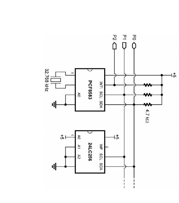
24LC256 EEPROM Schematics
 jean
Posts: 21
jean
Posts: 21
Hi,
Searching through the forum I noticed that there are different ways of connecting the 24LC256 EEPROM to the Basic Stamp
I would like to know which way is the most common if I wanna connect it to my BS2p40?
Right now I'm having problems with this sample code and this schematics without the PCF8583
Searching through the forum I noticed that there are different ways of connecting the 24LC256 EEPROM to the Basic Stamp
I would like to know which way is the most common if I wanna connect it to my BS2p40?
Right now I'm having problems with this sample code and this schematics without the PCF8583
bsp
2K
586 x 665 - 23K
Comments
I don't see any reason why you need the PCF8583.
I'm actually using the 4.7k resistors, I'm not using the PCF8583. I just had to use this schematics to make my connections
My question was about the A0 A1 and A2 pins. Do I make them high or low. I read that they are used for addressing but since I'm using only one EEPROM connected to my BS2p40 does the schematics work with my code?
I suggest changin your DevAddr to %000 and wiring your An pins to ground.
can I still work with this or do I have to desolder everything?
Or should I make modifications to the code?
thank you
Yes it says on the help file for I2CIN (SDA 0 or 8)
Now it works just fine