

Dynamic RAM

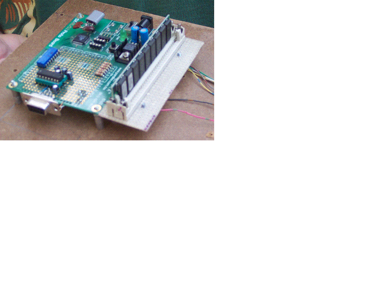
Here's a demonstration of an SX52 operating a dynamic RAM - a 30 pin SIMM salvaged from an old PC. This design should be able to access up to 32 megabytes of RAM.
I made this as an experiment to learn how to use DRAM and to see how suitable they might be to use·in a logger, and it worked quite well.
This demo uses a single 1 meg SIMM. It has routines to write to any individual address, read from any address, or to use it like a stack - write (push) to the next write address, or read (pop) from the next read address. And it does the DRAM refresh.
It includes RS232 send and get routines that let a PC communicate with the board. A few tests are built in - from a PC, you can send a character to the board to ask it to push a value to RAM, or send another character to pop from RAM and return the value to the PC. This way, you can push a few dozen characters, then pop them back to show the RAM is working. There also is RS232 code built in to run a Seetron LCD display. DRAM refresh is managed by the same ISR that runs the RS232 routines.
SIMM address lines are multiplexed into two parts, rows and column, of equal size. Since each address line is used twice, each additional line quadruples the capacity, rather than just doubling it. SIMMs come in 256K, 1, 4, and 16 meg sizes. 256K SIMMs have 9 pin row and column addressing, for 2^9 x 2^9 = 2^18 bytes, = 256K. So 256K needs 9 address pins, 1M use 10 pins, 4M use 11 pins and 16M use 12 pins. I used a 1 meg SIMM, but built the board to use all 12 address lines, so this design should be able to handle any of the sizes of DRAM.
The SIMM socket I used can hold two SIMMs. The column address strobe (CAS) is the chip select, so by using 16 meg SIMMs and two separate CAS lines, this same design should be able to control up to 32 megabytes of storage. But I haven't coded in the second CAS usage, or tried using 2 SIMMs. If 2 were used, the code would have to know when to switch over to the second CAS line, otherwise use of the higher addresses would just result in rolling over to point to address zero again. I measured that my SIMMs were 1 meg by testing for and detecting just this rollover.
When running from a 12V battery, at 20 mHz clock rate, the whole board draws 79 milliamps. Without the SIMM, it draws 74, so the SIMM itself seems to use about 5 mA at rest. I wasn't accessing the SIMM during this test, so I don't know if an active SIMM would be different.
I include a couple of documents that were helpful. But as I was learning how to do this, I also scanned the internet quite a bit and browsed many documents altogether to learn the general dynamic RAM process. But no single one of these other documents seemed comprehensive enough to include here.
My board includes a MAX232 to drive the RS232 to the PC. I used a 1K resistor array in the data bus to the RAM for protection in case I accidently set both the RAM and the SX data port to output at the same time. There are also resistors for protection of a few general purpose IO wires, one of which runs the Seetron LCD.
David

Comments
▔▔▔▔▔▔▔▔▔▔▔▔▔▔▔▔▔▔▔▔▔▔▔▔
"When all think alike, no one is thinking very much.' - Walter Lippmann (1889-1974)
······································································ Warm regards,····· G. Herzog [noparse][[/noparse]·黃鶴 ]·in Taiwan
Post Edited (Kramer) : 4/11/2006 9:11:14 AM GMT
This would be a great learning tool for computer electronics students.
Any, schematic's?
How fast can you read/write to the DRAM? Have you tested the throughput?
Thanks, PeterM
Wiring - The wiring is mostly direct from the SIMM socket to the SX data ports, as below. Sorry - I don't have a drawn picture of the wiring, but this should be enough info to build it.
I installed resistors of about 470 Ohms between port C and the SIMM data pins to limit current in case I were to accidently set both the RAM and the SX data bus as outputs during development, but these are optional. Also, a couple of good capacitors, like a 0.1 uf ceramic disc and a 10 uf Tantalum, probably should be placed at the supplies of the SIMM.
Google "30 pin SIMM pinout" and you'll see some nice pictures of the pinout.
Pin 1 is the end of the SIMM socket beside the alignment notch.
1 +5
2 CAS re.4
3 DATA 0 rc.0
4 ADDR 0 rd.0
5 ADDR 1 rd.1
6 DATA 1 rc.1
7 ADDR 2 rd.2
8 ADDR 3 rd.3
9 GND
10 DATA 2 rc.2
11 ADDR 4 rd.4
12 ADDR 5 rd.5
13 DATA 3 rc.3
14 ADDR 6 rd.6
15 ADDR 7 rd.7
16 DATA 4 rc.4
17 ADDR 8 re.0
18 ADDR 9 re.1
19 ADDR 10 re.2
20 DATA 5 rc.5
21 WE re.7
22 GND
23 DATA 6 rc.6
24 ADDR 11 re.3
25 DATA 7 rc.7
26 parity nc
27 RAS re.6
28 CASP nc
29 DPAR nc
30 +5
I used a dual SIMM socket. re.4 goes to the CAS of one socket, re.5 goes to the CAS on the second socket. All other corresponding SIMM pins are connected in parallel between the sockets.
David