

SX Addressing - Non Addressable Chips
 DigitalDj
Posts: 207
DigitalDj
Posts: 207
Hello,
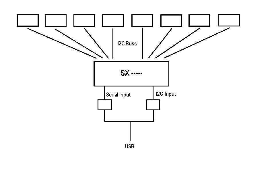
I would like to know if it is possible to input I2C signals into a SX chips input/output pins and have the SX chip select which 8 sets of I2C outputs to output to? The reason for this is to address 8 chips at any one time that are not addressable by software or hardware on the chip itself.·I have included a drawing.
Thanks,
Kevin
Post Edited (DigitalDj) : 7/8/2005 12:43:03 AM GMT
962 x 637 - 31K
Comments
Post Edited (Paul Baker) : 7/8/2005 4:00:04 AM GMT
to make things simpler, you can tie together the SCL pins of all I²C devices, and control them from one SX output pin. That is, you "only" need to use eight different SX pins to control the SDA line of each device separately. Of course, this only works as long as you communicate with just one device at a time.
You migt use one of the different available SX sample codes for an I²C master. I would suggest to add a subroutine which is called instead of setting/clearing/high-Zing the SDA line. The subroutine then takes care of controlling the right SDA pin.
▔▔▔▔▔▔▔▔▔▔▔▔▔▔▔▔▔▔▔▔▔▔▔▔
Greetings from Germany,
Günther
The chip i am wanting to address is the National LM4970, the more i look at the specs this chip has a address pin but the engineers at National says that it cannot be addressed as more than one chip. The address pin in the docs says it has 2 states X0 logic low and X1 logic high and is used to address a number of chips in a system, the LM4970's chip address can be changed to avoid any possible address conflicts. The way i take this is that the chip cannot be addressed as chip 1 thru 8 but can have all chips I2C lines tied together and the state of the address pins determine which chip can be addressed with I2C information!
I have·included the link·for the chip if someone would like to enlighten me as to how this works!
http://cache.national.com/ds/LM/LM4970.pdf
Thanks,
Kevin
·
Can you show me a diagram on that setup with and with out the 3:8 decoder?
On page 8 of the pdf it has EC for externally configered is this so each chip can be selected by outside means(master processor)
Thanks,
Kevin
·
to switch input I2C lines to 1 of 4 output I2C lines. The total lines required would
be 4 (SDA,SCL and 2 select lines). Just put 10kOhm pullup resistors on all
ingoing and outgoing I2C lines. You would connect 2 of your chips to each
outgoing I2C lines.
http://www.ee.washington.edu/stores/DataSheets/cd4000/cd4051.pdf
regards peter
▔▔▔▔▔▔▔▔▔▔▔▔▔▔▔▔▔▔▔▔▔▔▔▔
One remark, option C is not limited to the mentioned chip. You can use the same circuit
to address 4x8 = 32 PCF8574 chips for example. (You get 4 I2C buses).
regards peter
▔▔▔▔▔▔▔▔▔▔▔▔▔▔▔▔▔▔▔▔▔▔▔▔
Greetings from Germany,
G
that's true. So for option C, the 4052 could be replaced by a 4051 to give 8 I2c buses.
(requires 5 lines then).
regards peter
I am kind of new to these chips and to address them this way, i am also new to Sx programming!
Paul,
I have some questions on the drawings!
Drawing 1
1. The first drawing just has the address·lines coming from the SX and i would still have to tell the (8) LM4970's·address pins to·go low or high to address them?
2. Since the LM4970's have address pins does that mean that all (8) Lm4970's can run off of the same I2C buss and then when i want to address each chip i just set the address pin of that chip?
Drawing 2
1. Are all (8) of the LM4970's using the same buss in this drawing?
2.·Would i only·be able to address one chip at a time by multiplexing?
3. If i can use the same I2C buss for all (8) LM4970's·could i just use the SX without the mulitplexing chip for addressing the address pins of the LM4970's?
I guess if i wanted to use more LM4970's say 16 multiplexing would be the way to go!
Drawing 3
1. I don't understand·what's going on here with the CD4052, i need some explaination as to how this works.
Since i want to control this circuit from the USB port of the computer will that change any of these circuit ideas. The reason i want to control this circuit from the computer is it gives me more versatility. Also can i get a circuit to convert USB to I2C like the circuit from Parallax for USB to serial?
Sorry for all the questions!
Thanks!
Kevin
·
Figure
Figure C) The CD4052 is a true dual-channel 4-way multiplexor, its operation is equivalent to a DP4T switch (dual pole, 4 way throw), IOW·two switches which have four postions and the two·switches are set to the same position. So these are used to switch a single I2C bus on the SX side to one of 4 I2C busses that contain the LM4970s, the addresses of the LM4970s are set the same as in Figure A.
If you want·further explanation of what Geunther and Peter are talking about; ask, and one of us will explain.
The USB issue is another topic, so start another thread with that question. (It is a seperate issue that is unaffected by this issue)
Post Edited (Paul Baker) : 7/10/2005 6:23:09 PM GMT
http://www.i2cchip.com/
and scroll down to Host Adapter Products.
Check out the datasheet for the BL233 chip
and the ready to run I2C-2-PC USB adapter.
The USB adapter offers 3 I2C buses so you still
need a multiplexer to address all your 8 chips, but it relieves
you of interfacing to the USB bus.
regards peter
What do you suggest as being the best way to go?
If i wanted to add another 8 outputs what could i use besides the 138 or the CD4052?
Sorry for all the questions, i am just eager to learn and want make everything for the project i am working on! I want the circuit to control color modules designed and a proto made up to go where the white pastic is.
I have attached a picture of a Art Deco Jukebox i designed and building. I still have the button panel/hidden keyboard section to finsh up(getting close).
Kevin
Post Edited (DigitalDj) : 7/10/2005 9:34:26 PM GMT
at any time. If you want to address multiple chips simultaneously, you must have multiple
I2C buses that are serviced simultaneously.
You could dedicate an SX28 chip as follows:
port A (pins ra.0 to ra.3) = serial port with TX,RX,RTS,CTS
Use a max232 to connect to PC comport.
This can connect to a USB to serial adapter to allow control via USB
port B (pins rb.0 to rb.7) = 4x I2C bus
port C (pins rc.0 to rc.7) = 4x I2C bus
This gives you 8 independent I2C buses so you can connect 16 of your chips.
The code for the SX chip would consist of 8 master I2C routines, plus
a command routine that accepts commands via the serial port and dispatches
them along the 8 I2C buses. This can be done. The whole would be command driven,
meaning each I2C bus gets serviced when a command for that bus arrives.
regards peter
Could you show me what that would look like and would that be tough to program?
Kevin
·
You have to consider memory use first.
A I2C master running as Virtual Peripheral (to 'simultaneously' service the I2C buses)
requires 8 bytes, so for 8 buses that is 64 bytes or 4 ram banks.
Some buffering is necessary, assuming 4 bytes per bus, that is another 2 ram banks.
That leaves 2 ram banks for the serial port and command dispatcher. So it seems
to fit.
Using threads to run the virtual peripheral is a must here. If you have 4 threads,
during each interrupt only the Uart tx VP routine, Uart rx VP routine, and 2 I2C master VP
needs to be executed. That is doable also.
The command format you use, must allow you to select the I2C bus that you want to access.
Basically you need 3 commands:
B selects bus, B is followed by 0 to 7, eg. B 3
W writes data to chip on selected bus, eg. W F4·addr data (access LM4970 pin adr to GND)
R reads data from chip on selected bus, eg. R F6 addr (access LM4970 pin adr to 5V)
This is not a project you program overnight.·You must do it in assembly (due to the VP routines
and memory use). But it can be done. You might consider to do it in SX/B because that has builtin
commands for I2C master. But then the buses are serviced sequentially and I am not sure wether
that gives you enough memory.
regards peter
You could use that as a starting point. It also uses threading, so all functons you need are present
but you need to adapt it to your needs.
regards peter
1. I take it that the SX will only require 1 I2C bus on the input and then the controlled I2Coutputs through the SX?
2. How does the I2C buss know if there are more than 2 LM4970 on a buss if all chips are set high except the 1 that is low to be addressed?
3. If memory is a problem how about going with option C with the CD4052 or CD4051 that paul has described?
4. Am i correct in saying there is no provisions for the address lines to the LM4970's?
I guess for now if it is a real problem i could always stick with individual addressing to the LM4970's, processing speed would be great enough to probably not see any difference. The other problem is i will need to learn to program the SX but i guess that's the fun of it!
Kevin
are the 8 i2c buses.
2. You connect only 2 chips to each I2C bus. One of the chips must have it adr pin tied to GND,
the other chip must have its adr pin tied to 5V.
3. If you don't care about 'simultaneously' servicing the I2C bus, then you could program
in SX/B which has builtin I2C commands. As commands are executed sequentially, all I2C buses
can share the same memory. SX/B also has builtin commands for SERIN and SEROUT.
4. See 2.
regards peter
I must be missing something here, i thought the address pins also have to be controlled from high to low to send it information on the I2C buss! I thought that if i wanted to send information to chip one i would select it by bringing the address pin low and send the information on the I2C buss and then back high to address the next!
In Pauls drawing C·the LM4970's share the I2C buss and just the address pins are controlled, this is where i'm getting confused!
·Sorry This should have been drawing B
I'm kinda confused you might explain the how the I2C buss and the address pin on the LM4970 have to work together!
Sorry!
Kevin
Post Edited (DigitalDj) : 7/12/2005 3:00:06 AM GMT
Figure C does not show changing the address pins, see above for how the address pins are handled.
Here let me nutshell the issue and maybe you'll understand more clearly. You have 8 identical I2C devices you are looking to control. Those devices permit a maximum of two of them on an I2C bus that can easily be accessed. This is because they only provide a single pin to set the address so that address is either a 0 or a 1, no other possibilities exist. Now here is the crux of the problem, you have 8 devices which only permit 2 of them on a bus. So Figure A says: well if I have 4 I2C busses then I can access 8 devices with 2 on each bus. Figure C says: well thats alot of pins to use (8 devices, 8 pins), so what if I put a switch in there so that what appears to be a single I2C bus to the SX is actually 4 I2C busses that the switch switches between, now we have 2 pins for the I2C bus and two pins to tell the switch what position to be in for a total of 4 pins.
Now for Figure B, its probably best you forget about this one, it just seems to be confusing you, but here is another explanation. Figure B tosses the whole problem on its head, its looks at what can be done, even if the chips weren't really designed to be used that way. It says: ok forget about the number of I2C busses, what I need to be able to do is to access a particular device when I want to, thats all that matters. What if, instead of permanently setting the address of the I2C device like done·above, I make it so I can set the address of each device·during runtime.·So if I·can set the address of a device to a·0 while·simultaneously setting every other device's address to a 1, I can access that one device and my goal is accomplished.
I hope this is becoming·clearer for you.
Post Edited (Paul Baker) : 7/12/2005 12:02:58 AM GMT
Here is a little program I wrote in SX/B.
I can't guarantee it will work because I did not test it.
regards peter
Yes i understand what is going on now!
Also Thanks Peter for the program, if it doesn't work that's ok it still gives me a start! I'm sure i will be learning some programming for the SX and the whole circuit when done!
Peter,
Since the program is not setup to access all LM4970 at one time does that leave any memory for programming if i wanted to make the circuit stand alone without the computer control?
Regards,
Kevin
·
Most of the ram is available, as is page 3 and part of page 2, so there is room
for other tasks. Also note that port C pins and pins ra.2 and ra.3 are still
available.
regards peter
Which of the pins are the SDA and SCL on the 8 busses of the SX28?
Thanks,
Kevin
·
sda0 var rb.0
scl0 var rb.1
sda1 var rb.2
scl1 var rb.3
sda2 var rb.4
scl2 var rb.5
sda3 var rb.6
scl3 var rb.7
The builtin SX/B i2c command expect SDA on a even pin number, the SCL pin is then
automatically the adjacent pin.
regards peter
Thanks.
regards peter