

Occilator Location
 Armored Cars
Posts: 172
Armored Cars
Posts: 172
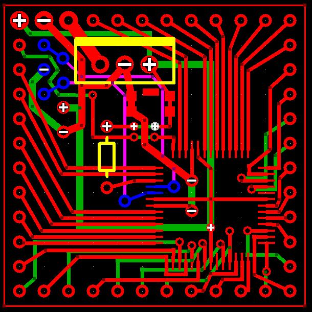
I'm working on an adaptor for the SX58 to make it thru-hole for prototyping stuff.· The only problem is I just read that the occilator should be as close to the chip as possible.· Could someone look at my drawing and see if the occilator location will be a problem?· The traces from the occilator are in blue (top layer) and pink (bottom layer).· It will be placed in the three holes to the far left.
Oh yeah, and if you see any other problems I missed please let me know.
Oh yeah, and if you see any other problems I missed please let me know.
610 x 610 - 96K
Comments
(Also, are you really doing this on a 4-layer board? That seems a bit generous - I suspect it would fit on 2 layers if you went with thinner tracks, and it's not as if 4-layer boards are easy to make at home...)
Steve
June 28th it should be available.
When I am done they should act as stand-alone chips, like a Stamp except with the power of an SX and built in reset button.
I wanted to keep the lines thick because I don't know how much power I will be using and would rather have the traces too big than too small. I might just make 12 with small traces and 6 the way it is now.
Well, I'll redraw this and post a pic when I get done. Oh yeah, Paul Baker I couldn't figure out how to use that file.
▔▔▔▔▔▔▔▔▔▔▔▔▔▔▔▔▔▔▔▔▔▔▔▔
I'll have to wait until school starts to get the sparkfun programs downloaded and redraw it then.· (We have 28.8 Kbps dial-up)· When I redraw it I will run all the traces exactly as they are in this pic.
A few other things about the layout, your concern for trace width is unessesary, an SX pin can only conduct 25 mA safely, a 1 inch 8 mil width trace can carry 1/2 amp and only raise in temperature 1 C. The only traces you should have wide is the power traces.
And if your layout software can make flood filled areas you should make the entire back flood filled ground (it will route around your signal traces).
Pin #1 should come off parallel, not at an angle, the odd layout you have can create electrical "echo chambers", it is so short that its resonancy is probably in the gigahertz but its better to be safe.
If you reroute the trace going to the top pin of the oscillator so that it loops under and around the second pin your need for more than two layers disappears.
On your I/O lines try to avoid 90 degree turns, this can create reflections in the signal.
It appears some leads will solder to pads, while ohther leads will solder to traces, was that your intent?
Here is a couple excerpts of my last board using an SX52, I don't claim its a perfect layout but I did spend considerable effort researching and thinking about the layout. The first is a photo without flood fills shown, its easier to pick out the components. #1 is the SX, #2 is the oscillator, I placed this further away because it is an actively driven oscillator which can be placed further from the processor, you are using a resonator which relies upon the SX to drive it so it must be placed closer. #3 is an SPDT switch to switch between the oscillator and the SX-Key header, an actively driven oscillator and the SX-Key must not drive the OSC line simultaneously because the oscillator will damage the SX-Key. #4 is the SX-Key header to program the SX. #5 is the reset button and #6 is one of the 4 bypass capacitors of the SX to reduce ripple in the power supply.
The second picture shows the flood filled areas, the blue is the backside ground plane, and the red underneath the SX is a Vdd flood fill on the top side of the board. The ZOhm resistors are zero ohm resistors (a jumper) to connect areas of the ground plane which are broken up by the Vdd traces, you want to provide as close of a direct loop for power as possible, the Vdd and Gnd going to each component should be as straight of a shot to and from your power source as much as possible. (My power jack is just off-screen to the bottom right)
Perhaps these examples can help illustrate some of the points I was making.
Post Edited (Paul Baker) : 6/23/2005 3:13:04 PM GMT
No 90 deg. turns
No short little pieces like on pin 1
Smaller traces (for 25mA max)
Thanks!
Two things strike me about your layout:
1. It won't work on a typical breadboard. How were you going to use this? I ask because...
2. The pins in the three border pins in the upper left are considerably larger then the rest of the border pins. If the majority of these holes are designed for the typical 0.025" wirewrap pin, then those three larger holes are the "odd men out", size-wise.
It's been a while since I did wirewrapping or much work on tenth inch prototyping boards. I'm about due for a revelation.
Later!
kenjj
JT
Post Edited (Miner_with_a_PIC) : 6/26/2005 2:00:00 AM GMT