

Silly Electronic question
 Beau Schwabe
Posts: 6,576
Beau Schwabe
Posts: 6,576
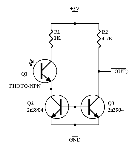
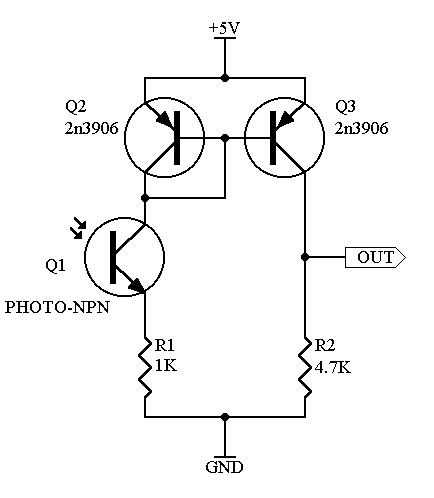
Ok, so I know the answer to this (I think) but I had a rather lengthy
discussion with a co-worker of mine that insists that the two circuits
below are fundamentally different. With the exception that one provides
an inverted output compared to the other one, I personally do not see a
fundamental difference... Am I missing something? Also, this person
swears up and down that you can not swap R1 and Q1 and expect the
circuits to function the same.... At this point I realized this would be a
moot argument.
▔▔▔▔▔▔▔▔▔▔▔▔▔▔▔▔▔▔▔▔▔▔▔▔
Beau Schwabe - Mask Designer III
National Semiconductor Corporation
Latest Company News
(Communication Interface Division)
500 Pinnacle Court, Suite 525
Mail Stop GA1
Norcross,GA 30071
442 x 499 - 6K
434 x 498 - 6K
Comments
Yep, I see no fundamental difference, it's all symmetrical, as you suggest.
A quick LTSpice run (.asc available, if you care), with 2N2222s with current injected into the base (I can't think of a better way to easily model a phototransistor...) says that they're pretty equivalent, too.
As for swapping R1 and Q1, I guess that depends where the light is arriving on the PCB [noparse]:)[/noparse]
Steve
Take into account that this person is a circuit designer (scary thought), and does
not deal with Bipolar transistors day-in day-out... mostly just CMOS transistors.
This person claims that the NPN version is not of a "conventional circuit" whatever
that means and that it shouldn't work at all like the PNP version inverted or not.
(a little background) .....Originally when I asked a question about the circuit it
was in it's NPN form. My co-worker proceeds to draw the PNP version, to which
I exclaim that "they are functionally the same". From here the silly argument
that started debate began.
SteveW,
I might be interested in looking at your .asc The light source to the phototransistor
is about 60Hz 500uS wide pulses, modulated with a 31kHz carrier.
As far as swapping R1 and Q1... I told my co-worker that I might be able to see a
problem if the components were sitting on the same substrate such as in a CMOS IC
design, but since the components are discrete devices there would be no substrate
sharing, and this would not be an issue.
▔▔▔▔▔▔▔▔▔▔▔▔▔▔▔▔▔▔▔▔▔▔▔▔
Beau Schwabe - Mask Designer III
National Semiconductor Corporation
Latest Company News
(Communication Interface Division)
500 Pinnacle Court, Suite 525
Mail Stop GA1
Norcross,GA 30071
Nope - I'll try and zip it.
Yep - that seems to have worked. There are .wmfs of the schematic and the plot, too.
Steve
(Oops - uploaded a duff old version the first time. If you got the one with current sources from B<->E, rather than capacitive voltage sources, on the phototransistors, you're safe. )
Steve
(These are definitely discrete devices being modelled - no substrate or any other integrated stuff going on)
Post Edited (SteveW) : 3/23/2005 5:05:21 PM GMT
Did this disagreement hinge on schematics drawn on beermats? [noparse]:)[/noparse]
Steve
More likely the case... This person is "technically" the only circuit designer
here at this facility. Since I pretty much only do IC layout (build the resistors,
inductors, capacitors, diodes, transistors, etc. from the schematics the designer
hands to me), it is easy to forget that there are other people fully capable of
design. It will definitely shed some light on how I will perceive this persons
abilities in future applications when I receive a schematic to work on.
This thread was more of a sanity check.... I thought I might have overlooked
something that should have bit me. Thanks for the input!
▔▔▔▔▔▔▔▔▔▔▔▔▔▔▔▔▔▔▔▔▔▔▔▔
Beau Schwabe - Mask Designer III
National Semiconductor Corporation
Latest Company News
(Communication Interface Division)
500 Pinnacle Court, Suite 525
Mail Stop GA1
Norcross,GA 30071
the only minor difference i see in the ckt is (and i could be wrong here):
with the npn ckt
+5v - VR2 > Vout > Vce - GND
with the pnp
+5v - Vce > Vout > VR2 - GND
right?
▔▔▔▔▔▔▔▔▔▔▔▔▔▔▔▔▔▔▔▔▔▔▔▔
League Bowling.... it's not a sport, it's a way of life
I would not consider him green, but I think he likes to argue...
You are correct, thus the inversion between the two. The output varies slightly
from the function of R2 configured as a pull-up or pull-down and the .6V rail limitation
through Q3.
▔▔▔▔▔▔▔▔▔▔▔▔▔▔▔▔▔▔▔▔▔▔▔▔
Beau Schwabe - Mask Designer III
National Semiconductor Corporation
Latest Company News
(Communication Interface Division)
500 Pinnacle Court, Suite 525
Mail Stop GA1
Norcross,GA 30071
▔▔▔▔▔▔▔▔▔▔▔▔▔▔▔▔▔▔▔▔▔▔▔▔
G. Herzog in Taiwan
Also, these circuits are using a current mirror topology. That is something that works very well in integrated form but is not very good in discrete form. When on the same die, the two current mirror transistors are at the same temperature and have had the same processing. That is not true of the discrete parts shown. Neither would be very good circuits for production in discrete form.