

SXploded
 Guenther Daubach
Posts: 1,321
Guenther Daubach
Posts: 1,321
Hi,
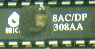
did·you ever want to take a look inside of an SX28?
One of my customers must have connected the Vdd and Vss pins directly to a wall outlet ·which made part of the plastic cover blast away. So I can now look at·some part of the chip inside.
I have attached a photo - hopefully it will upload and show enough details.
Greetings,
Guenther
▔▔▔▔▔▔▔▔▔▔▔▔▔▔▔▔▔▔▔▔▔▔▔▔
Post Edited (Guenther Daubach) : 7/26/2004 5:56:45 PM GMT
did·you ever want to take a look inside of an SX28?
One of my customers must have connected the Vdd and Vss pins directly to a wall outlet
·which made part of the plastic cover blast away. So I can now look at·some part of the chip inside.I have attached a photo - hopefully it will upload and show enough details.
Greetings,
Guenther
▔▔▔▔▔▔▔▔▔▔▔▔▔▔▔▔▔▔▔▔▔▔▔▔
Post Edited (Guenther Daubach) : 7/26/2004 5:56:45 PM GMT
389 x 203 - 56K
Comments
Click edit button on the upper right of the message in question and make the corrections directly to the test.
HTH,
Daniel
▔▔▔▔▔▔▔▔▔▔▔▔▔▔▔▔▔▔▔▔▔▔▔▔
---
James Newton, Host of SXList.com
james@sxlist.com 1-619-652-0593 fax:1-208-279-8767
SX FAQ / Code / Tutorials / Documentation:
http://www.sxlist.com Pick faster!
thanks for making me aware of the edit button. In the meantime, I have tried it out, replaced/added the wrong/missing characters in the original message. While doing this, I also came across the "Delete Post" button, so I used it to delete my other message which has become obsolete now.
I like these fine features!
G
I tried my very best to enlarge the picture as far as possible, and setting my DigiCam to its maximum resolution. Let's see if I can find a microscope somewhere around here...
G
edited:· You might try placing the chip on a flatbed scanner, and scanning at high resolution.
▔▔▔▔▔▔▔▔▔▔▔▔▔▔▔▔▔▔▔▔▔▔▔▔
00000000000000000000000000000000000000000000000000000000000000000000000000000000000
this is a great idea, I've just scanned it @ 1200 dpi - the result is attached.
G
How about a caption contest ?
"I told you it wouldn't run at 50 GHz"
"Trying to power the arc-welder from a single pin was probably a bad idea"
"That line-voltage transformer WAS optional wasn't it"
Bean.
Regards,
Al Williams
AWC
http://www.awce.com
I like your "That line-voltage transformer WAS optional wasn't it" caption most.
Hi Al,
Im sure your methods for taking a closer look to the inside of a chip are much more precise, allowing to exactly select the layer you want to inspect but the method my customer used does not require any toxic chemicals at all, so this is a good alternative for private tests at home. Although I cannot guarantee that the results will always be the same when connecting the Vdd and Vss pins to a wall outlet. I have another SX-28 here that was installed in the same system which simply created some smoke without blasting away the epoxy above the die before going to semiconductor's heaven.
Greetings,
G
▔▔▔▔▔▔▔▔▔▔▔▔▔▔▔▔▔▔▔▔▔▔▔▔
---
James Newton, Host of SXList.com
james@sxlist.com 1-619-652-0593 fax:1-208-279-8767
SX FAQ / Code / Tutorials / Documentation:
http://www.sxlist.com Pick faster!
hard to believe that this thread still holds the record for the most views.
Maybe, I should try to blast some more SXes to get an even better view of the inside.
On the other hand, as we have an expert in this thread, it might be the better idea to ask Al if he could "dissect" an SX for us.
Greetings, G
A dremel in a drill press stand would do to make the cavity, but I would not suggest anyone handle fuming nitric without a vent hood.
Of course, if you have a UV erasable part (not an SX, obviously) you can usually pull the window off of them with an X-acto knife.
Here's a small chip that was never encapsulated (that's another easy way to look inside).
Al Williams
AWC
I certainly see a seam on the SX IC.· Just food for thought.
ken
I've got a dremel here, and a drill press stand, and I also have another SXploded here, so I'll give it a try :-).
G
We used to also make our own microprobe needles using Sodium Hydroxide and an isolation transformer. One lead of the transformer went into a beaker of the Sodium Hydroxide. The other lead clipped to a piece of steel rod. You'd plunge the steel rod into the solution. Say the tip went in at T=0. As you continue down, the tip is still under at T=1 and, say .25 of the rod is in the solution by this time. at T=2, .5 of the rod is in solution, the tip has been in for 2 time units, the .25 mark has been in for 1 time unit, and the .5 mark has just gone in. As you pull the needle out (assume the same speed) then the tip was in for T=4, the .25 mark was in for T=3, and the .5 mark was in for just an instant. That means that more is eaten away at the tip then the shank, and the rest of the rod gets eaten away in proportion to its nearness to the tip. A few dozen plunges makes a wonderfully sharp microscopic needle.
▔▔▔▔▔▔▔▔▔▔▔▔▔▔▔▔▔▔▔▔▔▔▔▔
---
James Newton, Host of SXList.com
james@sxlist.com 1-619-652-0593 fax:1-208-279-8767
SX FAQ / Code / Tutorials / Documentation:
http://www.sxlist.com Pick faster!
while the image on the left is a cell-block that I just completed.
▔▔▔▔▔▔▔▔▔▔▔▔▔▔▔▔▔▔▔▔▔▔▔▔
Beau Schwabe - Mask Designer III
National Semiconductor Corporation
(Communication Interface Division)
500 Pinnacle Court, Suite 525
Mail Stop GA1
Norcross,GA 30071
Cool stuff. So, is this actually a complicated chip or does it just look that way? I ask because it looks like a ton of stuff going on in there, but I wasn't sure if this was one of the hard ones or the easy ones.
Thanks,
PeterM
When you have guys like Al Williams "grading" your work, ALL chips are difficult - grin (Sorry Al)
....Seriously. I'm not exactly sure what would be considered easy about a chip. All of them have
their obstacles that the designers and layout people must overcome. It is a very tedious effort, and
at times can be extremely frustrating. I myself enjoy the challenge....If it was easy, then I would
probably be doing something else.
▔▔▔▔▔▔▔▔▔▔▔▔▔▔▔▔▔▔▔▔▔▔▔▔
Beau Schwabe - Mask Designer III
National Semiconductor Corporation
(Communication Interface Division)
500 Pinnacle Court, Suite 525
Mail Stop GA1
Norcross,GA 30071
Is the layout still done, or at least checked on VERY LARGE sheets of paper?
I had a short stint at an IC joint (Linfinity) and remember the engineers doing layout on HUGE pieces of paper.
It was also facinating to me the machines that would test the wafers for good vs bad "modules".
That machine was fast..
And then the almost assembled IC without the lid, mounted on an XY table fitted with a microscope and probes to measure voltages inside the little beast.
Ken
the one that we have used requires that each layer or "Mask" is printed to a glass template
where it is optically scaled. There can be many different layers for this process. Another
approach uses E-beam (Electron Beam) which deposits metal onto the chip.
I'll have to admit, the fabrication process is a little vague to me, so forgive my limited answer.
▔▔▔▔▔▔▔▔▔▔▔▔▔▔▔▔▔▔▔▔▔▔▔▔
Beau Schwabe - Mask Designer III
National Semiconductor Corporation
(Communication Interface Division)
500 Pinnacle Court, Suite 525
Mail Stop GA1
Norcross,GA 30071