

4 layer boards, power distribution, high speed signaling, and cross talk
 ke4pjw
Posts: 1,334
ke4pjw
Posts: 1,334
So, in 2021-2022 I designed a pixel light controller board with the P2 Edge. It has one fatal error. I chose to do a 2 layer board and I did a pour for the ground. Everything appeared to work great, until I started using ports 17 - 24. As soon as the cog that runs those ports started, I would get glitches in the pixel outputs, on other ports. What was suggested was to change the drive level of the outputs to be lower in the pin settings. The alleviated 99% of the problem. The island I had on the ground pour made the problem worse than it needed to be. I would have done better by not placing it there at all.
This year I started using all of the ports on a couple of my controllers and intermittently, port 21 will glitch. It appears that it is the victim and the ethernet traces are the aggressor. I have wanted to do a redesign, and this is my opportunity to fix it. Additionally, I hope to improve my throughput and remove some of the waits I had to add when communicating with the Ethernet chip.
My plan is to not use the Edge or Wiznet Ethernet boards. Do a full layout and place all of the components on a single board. In order to accomplish this, I believe I will have to do a 4 layer board. They are not that much more expensive from what I can tell. Using a 4 layer board allows me to have 2 power planes with one acting as a ground/return plane. This is my thought for layout and use of those layers:
Top Layer 1: All ICs mounted up top on this layer. All high speed traces (such as ethernet) on this layer. Power supply + rails on this layer.
Layer 2: Ground, full pour, except under ethernet magnetics.
Layer 3: +VCC this layer, full pour, except under ethernet magnetics. Possibly some Power supply rail distribution. There are no analog sections of this board.
Bottom Layer 4: Low speed traces on this layer. ie Display and ws2811 signal distribution.
Does this appear to be a good strategy? Any unsolicited advice is appreciated.
--Terry
Comments
First a couple Q's...
What's the top clkfreq?
Also... Might be lacking enough ground plane to act as the heat spreader. Are you thinking of using a fan and/or heatsink?
270MHz on the P2. Comms to the ethernet, well, that will be interesting. I am going to wire it for both SPI and parallel and see which can be made to deliver faster throughput. SPI Clock 70Mhz (max) and Parallel, maybe, 25Mhz?
For P2 cooling, I was thinking of just using VIAs on the groundpad to help distribute the heat to layer 2. Similar to what is done on the Edge.
4 layers is probably overkill but should solve any issue like this.
I never really had a problem with 2 layer until this attempt at a Mega compatible board that was very noisy, as I recall.
I think the reason is that the ground plane was horribly infiltrated with wires, making it a very bad ground plane.
Seems the usual thing is to make inner layers power and ground. But, for EMI, power is same as ground.
For my SimpleP2 boards, I have one inner layer as mostly 3.3 V and the other as mostly 1.8 V.
@ke4pjw Just looked at your board in other thread and think I do see similar ground plane issues as shown here...
One trick for two layers is to try to have wires only going in one direction on top plane and other direction on bottom plane.
Helps to preserve the ground plane...
It could be a ground bounce problem. The Edge has 3 ground pins out of 80 total pins, and they are all grouped together. Only 4%. I can't imagine the edge module crashing, they are 6 layers now, right? Adding bypass capacitors on the mainboard for the Vio pins might help a little bit.
PCI 18 of 114 pins are ground 16%
Raspberry Pi 8 of 40 20%
i've made some 2 layer P2 boards. I can't really comment on the reliability. I run them at 80 MHz and most of my signals are analog inputs. It's a little tricky to fan out the signals and connect all the 3.3v pins and maintain a relatively unbroken ground plane. It might be easier to do a 4 layer board.
Yeah, the first board has problems due to the partial islands highlighted in blue. Especially the center one. Those are unintended antennas")
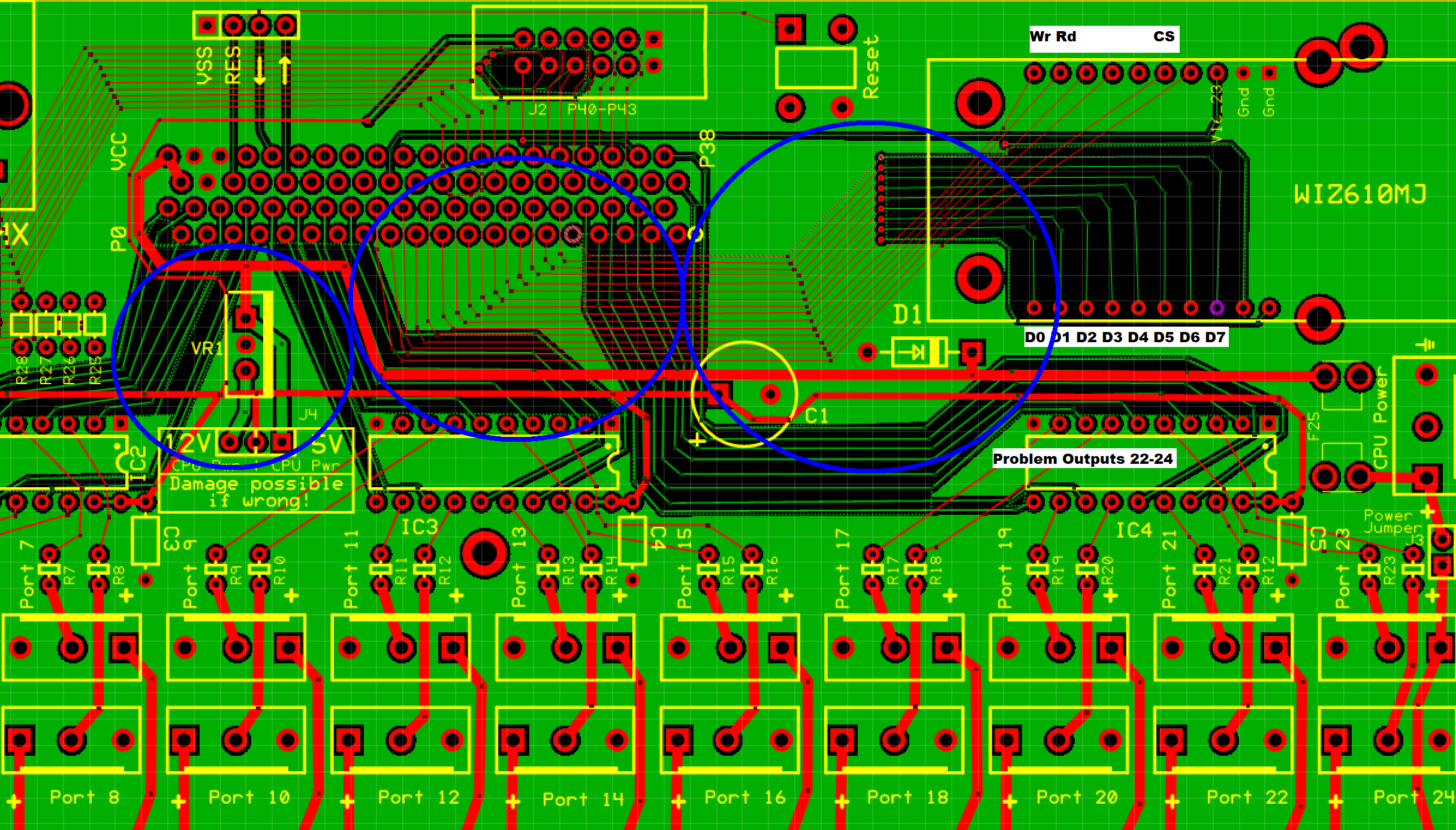
I have been reading the book PCB Design and Layout Fundamentals for EMC and watching videos on crosstalk. I now know that those partial islands grounded on one side are worse than not having anything there.
The problem with multi-layer boards is you can't "see" how things are routed and I wasn't sure if how I am stacking the layers is the right approach or not. The one book and handful of videos I watched make me feel like I am doing it right. Just hoping the more experienced folks in the forums could weigh in.
As you and others mentioned going to 4 layers and getting a ground plane in between (on either internal layer) will sort this out. However there's a lot you could improve while still in 2 layers
I was lucky enough to do the PCEA circuit board professional course earlier in the year and they talked a lot about the evils of separated/interrupted ground pours. Mike (the same PCEA instructor) talks about it in this public Altium video around the 41m mark, https://youtu.be/3Is7bra3tsc?t=2459.
From a practical 2 layer point of view, the place to start would be to get copper pours in between each of the vertical green signals. While its possible to just bunch the green really close, that might introduce tighter coupling between those signals and their neighbours, so ground islands in between would be better. It might be possible to get the ground into that area by changing the ground pour boundary from the IC4 end, but I suspect you'll need to have a ground trace ("crossbar") running horizontally on the red layer near the P2 edge connector, and a single via down to each ground island below on the green layer.
The next thing to do is provide a tight ground return for the clock on the red layer, especially where it crosses the separation in the green ground pours. It can just be a single trace, or a couple of traces above/below the clock.
Thanks @Tubular! That video looks great! Definitely one I will watch over the holiday before I start layout on the new board. I am not going to attempt to fix the old board. It is locked with a proprietary vendor who has to build the initial boards, before they give me gerbers. I have since learned KiCad and will be doing layout in it. The cost of 4 layer is not that much more than 2 layer. Might as well make things easy on myself.
That PCEA training looks very interesting. Would it be of any value to a novice? They have classes close by (in GA). Cost is similar to what I paid for my vmWare training a decade ago. (also was a week long class in GA) I might pony up for that, even though I am a hobbyist. I really enjoy this stuff.
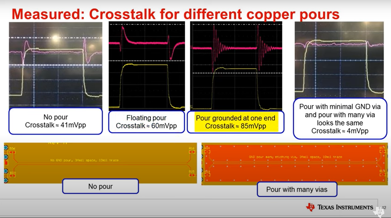
Something else that really drove the issue of crosstalk home for me, is this image from the book I am reading.
Since these are pulses, the return current follows the path of least inductance, not resistance.
I've been using 3 different pcb packages this month and its Kicad thats certainly coming along in leaps and bounds. Yes, 4 layer is really the way to go in order to not have to deal with these kind of issues. There are many benefits including accessing finer track and space clearances, and you're right, its not really that much more expensive
With regard to PCEA and novices, I've gotta say "not really". Its really geared towards higher speed fpga-like multilayer board design where lots of things really matter. That's not to say there's not plenty of interesting stuff along the way, and I sure learned a lot about how pcbs are made. But the Altium academy and youtube cover a lot of this material for free, so thats where the value really lies for a novice. I think where it would be of most value would be anyone about to embark on BGA (fpgas, high pin count processors etc)
That info you found regarding low and high frequency paths is interesting isn't it. In the video I posted Mike talks about wrangling/managing the field between a high speed signal and its return, and the area in between that it spans. You basically want to keep it constrained so it doesn't cross couple as much. Rick Hartley also talks about this in his videos.
Well, I now have a more interesting problem, and I think it can only be resolved with software. I want to maintain the high speed integrity of an 8 bit data bus between my ethernet chip and a P2. The problem is, the MSB and LSB are swapped where the lines would meet each other if a straight signal path is drawn. I can't come up with a placement geometry where I don't use a via to swap the lines. I am thinking I may have to add an instruction to swap the bits in software. Any suggestions?
Can you not just rotate the ethernet chip around? But a few vias should be fine for P2 signalling speeds. That 96MB PSRAM board I use a lot has somewhat awful routing and lots of vias (and is of course an external board that plus into an EVAL), yet it's still fine at ~100 MHz (but not 150 MHz anymore). Your CAD package should be able to create impedance-matched tracks, which may(?) also improve performance.
@Wuerfel_21 The only way I can get it to work with a hardware solution is to use vias. Everytime I turn the chip it still oriented wrong. I suppose I could carve out space on the power plane and do it there. It would be further away from the ground plane than I would like. Might be better to go all the way to the bottom. It would be coupled to the power plane then.
Seems like this would be a common problem for high speed circuits. I was not wanting to compromise, but I don't think I have a choice, unless I flip the bits in software. I can certainly spare a cycle and I bet there is a single instruction to flip the bits.
Surface mount actually helps out a little here. Without the through holes, there is more board space for vias. And vias are often needed anyway just to route the signal tracks under the power and/or ground rings.