

QSPI driver for LAN9252 [solved]
 ManAtWork
Posts: 2,369
ManAtWork
Posts: 2,369
(title was: "looking for SQI driver")
I haven't found anything in the OBEX but I think somebody has already implemented a driver for SQI (4 bit wide SPI) for some external memory chip.
I don't need extreme speed but using smart pins and ~sysclk/4 would be nice.
Comments
There is various incarnations of testing done using a Streamer for 4-bit PSRAMs. They are all geared for speed. I never finished anything, Roger Loh has a big-Smile driver, Rayman might have something smaller.
Doing that with smartpins is burdensome for a couple of reasons: The clocking feedback becomes clumbersome above two bits, you have to put the clock pin in the middle of the data pins. And massaging the four serial smartpin streams to act like one parallel stream takes a bunch of instructions that caps the top speed. Amusingly multi-bit SPI is not serial at all.
@rogloh does have a nice driver that I've been using as one of the codes to test my boards with.
It appears to have all the bells and whistles you'd ever want.
I do want to work on my own version though. Thinking about using two, 8-bit, banks to do double buffered video.
Also want to see if SQI flash can share the busses...
Was hoping to work on this over the holiday break, but there are some other things needed to be done first...
I need to interface to a LAN9252 which behaves basically like a small dual-port RAM. But instead of doing large block transfers like for video buffering I'm expecting to do many small reads and writes. I think using the streamer is too much overhead. Luckily, I've already put the clock pin in the middle between the data pins. The SPLITB and MERGEB instructions should do the job of seperating and combining the four bits.
The video and RAM drivers are highly specialized so I think I have to roll my own, anyway. But it's always easier to look at something that already works than starting totally from scratch.
Maybe SQI is overkill and not much faster than single bit SPI. Having to re-configure the data pins for in and output is probably more overhead than having a MISO/MOSI pair with fixed direction. So it pays back only for large transfers.
Oops, kind of forgot the most annoying part of using Smartpins: Sysclock/4 is way faster than the latency of the I/O staging. This badly impacts sync serial tx mode due to both the input latency and output latency stacking onto the clocking. Sysclock/4 is possible, and is fastest possible at all, but even sysclock/8 is too fast for normal clock-data relationship. To get sysclock/4 requires customising it for exclusively sysclock/4. No other divider will work then.
An option would be to use bit-bashing or Streamer for tx function and use Smartpins for rx function. That would avoid the latencies in both directions and in theory can flexibly go any divider.
Looks like I did exactly that with the EPPROM boot code that was in use for a while. It got dropped because not all EEPROMs supported the DualSPI mode I had programmed it for.
It's only doing 1-bit bit-bashing for tx since that was all that was needed. That could be improved. The clock-gen can be made a common smartpin for a starters.
'------------------------------------------------ send_byte2 shl pa, #32-7 wc rep @.loop,#8 outc #spi_di outh #spi_clk shl pa, #1 wc outl #spi_clk .loop ret '------------------------------------------------ read_byte4 waitse1 'wait for smartpin (spi_do) buffer full event rdpin pa, #spi_do '16-bit shift-in as little-endian (odd bits) rdpin pb, #spi_di '(even bits) rev pa 'but SPI data is stored as big-endian (odd bits) rev pb '(even bits) rolword pa, pb, #0 'combine to a single 32-bit word _ret_ mergew pa 'untangle the odd-even pattern '------------------------------------------------Here's a snippet of 4-bit Streamer code I wrote. All it does is send a QPI/SQI command as two nibbles. It, and two others, were developed as general routines but do depend on a lot of compile time timing calculations. Particularly for the M_LEADIN constant, which can handle many config settings like clocking mode and pin registration.
PUB tx_cmd( cmd ) org setxfrq xfrq ' set sysclock/1 for lead in timing rolnib cmd, cmd, #1 ' big-endian nibble swap drvl datp ' drive the data bus for CA phase drvl #PSRAM_CE_PIN xinit leadin, #0 ' lead-in timing, at sysclock/1 setq nco ' streamer transfer rate xcont ca4, cmd ' tx Command only dirh #PSRAM_CLK_PIN ' start smartpin internally cycling at SPI clock rate wypin #2, #PSRAM_CLK_PIN ' 2 SPI clocks for Command only waitx #2 * CLK_DIV - 4 dirl #PSRAM_CLK_PIN ' reset smartpin dirl datp ' tristate the data bus upon completion _ret_ drvh #PSRAM_CE_PIN xfrq long $8000_0000 leadin long M_LEADIN nco long M_NCO ca4 long M_CA4 datp long PSRAM_DATA_PIN endOf note is it uses one smartpin for external clock gen.
There is a small headache with timing the streamer against a smartpin. The two pulse gen smartpin modes, that can be used for this, both have the same quirk - Pulse cycle timing is aligned to DIR rise, irrespective of if pulses are generating or not. This means that when WYPIN issues a fresh count of pulses, the smartpin still waits for the completion of prior cycle before producing its first pulse. And what's more, a WYPIN is ignored while DIR is low so DIR must be raised first.
Streamer commands don't do that thankfully. They act immediately if a command is not already operating.
So this all means the software has to account for the smartpin's behaviour and align the streamer startup to match the smartpin pulse gen. That's what is going on here. "leadin,#0" is pacing out the streamer with empty bits to make the real "ca4,cmd" bits start later. After the streamer is setup, then the clock gen is started with the DIRH-WYPIN paired tightly together. By keeping them paired together allows one instruction order for all clock dividers.
xinit leadin, #0 ' lead-in timing, at sysclock/1 setq nco ' streamer transfer rate xcont ca4, cmd ' tx Command only dirh #PSRAM_CLK_PIN ' start smartpin internally cycling at SPI clock rate wypin #2, #PSRAM_CLK_PIN ' 2 SPI clocks for Command onlyThe full source code also handles paralleling of multiple PSRAM chips so it can handle up to 16-bit transfers across four ICs - Which of course suits the EC32MB Edge Card.
Hmm, I seem to have multiple versions. The one above I remember was the development name. All my testing was done with it, so it could have been left incomplete. I also had it working with 8-bit and hyperbus parts too. Here's one that is named for 4-bit wide ICs. The differences are only in the details, and to be honest I don't know which is more complete.
EDIT: Added the required "stdlib.spin2" file.
Oh, more recently I experimented with pretty much every combination to do full SD card support ... kind of forgotten about at some point. I should have had that completed already ...
Here's a rough snippet of code that uses a smartpin for CMD tx out. So only 1-bit serial. It uses two timing options to handle either sysclock/4 or greater than sysclock/5. So I was a little wrong about sysclock/4 requiring a special code path. Its limitation is that it needs the data delay that CPHA=1 provides. So only cmodes 1 and 3 can be supported.
    uint32_t  crc = (0x40 | cmd)<<24 | arg>>8;

    _pinf( PIN_CMD );    // reset tx shifter
    _wrpin( PIN_CMD, P_SYNC_TX | P_OE |    // setup CMD output smartpin mode
            (PIN_CLK - PIN_CMD & 7)<<24 | (CMD_DIV<6 ? P_INVERT_B : 0) );    // SmartB input (CLK pin)
    _wxpin( PIN_CMD, 31 );    // 32-bit shifter, continuous mode
    _wypin( PIN_CMD, _rev( crc ) );    // first 32 bits into tx shifter, continuous mode

    _pinf( PIN_CLK );    // cancel excess clock gen
    _wxpin( PIN_CLK, CMD_DIV | CMD_DIV/2<<16 );    // set SD clock rate
    _pinl( PIN_CLK );
    _wypin( PIN_CLK, 6 * 8 );    // begin SD clocks, tx smartpin won't see clocks for about 8 sysclock ticks
    _pinl( PIN_CMD );    // start tx shifter, in continuous mode
It's a little out of spec at higher dividers (eg: 20) though. That option is actually clocking the tx data out on the rising clock edge. It suits sysclock/8 because it takes four ticks of lag (From the latency of the I/O stages) for the tx data to appear in response to the clock.
Which is why the alternative requires the CPHA=1. It needs to be clocked on the prior falling clock edge. A whole clock cycle earlier than produced at the pin. Which, for a divider of sysclock/4, the same lag of four ticks fits perfectly.
Don't use pin registration when using the sync serial smartpins. That would increase the number of I/O stages and therefore also the lag effect.
Oops, yes, this is going to get tricky. When developping the SPI driver for the LCD I managed to balance out the latency quite well by using sync mode and inverting the B input (clock). But that ran at only 20MHz = sysclock/10. If there are asynchronous routing delays considerably longer than one clock they will have an impact at sysclk/4. I definitely want to avoid overclocking above 200MHz and having to adjust the delay for each board individually is also no option. So running at a lower frequency and with as much bits in parallel as possible is definitely better than trying to hit the max frequency.
Cleanly phase aligned at sysclock/4 is possible via cmode = 3 (assuming the LAN9252 accepts cmode 0 and 3) and a non-inverting tx clock input. This is what you'd see from the tx pin:
Err, um, clock input inversion can be for two reasons. Both CPOL and latency compensation affect it. What I've at least done once is apply CPOL at the SPI clock pin low-level input as well as output. This then presents a positive polarity internally irrespective of CPOL setting so any timing adjustment is then applied to individual smartpins as if no CPOL inversion is present.
My SD testing C code snippet above doesn't do this. It is using cmode 3 but only inverts the SPI clock output. The low-level input is non-inverting. Hence it inverts the tx smartpin B input when divider is less than 6, rather than the other way around.
I never used the streamer, really, but isn't there a way with the eggbeater to align the clock exactly to the clock smartpin? i would like to understand where the problem with the sysclock/4 lies...
Streamer alignment is because of the way those clock gen smartpin modes cycle. Trying to use hubRAM accesses to align the timing would be highly ill advised. Just changing a hub address will throw a curve ball. Roger and others, and myself historically, have used coincidence of instruction counting against smartpin cycle. Which works as long as the divider is a singular hard-coded ratio. My method above allows for a compile time divider setting.
Sysclock/4 shenanigans is due to the number of inline flip-flops (stages) in the I/O signal path internal to the Prop2. There is a write up on this in the newer Hardware Manual, under the section I/O Pin Timing, dealing with the large number of stages between the Cogs and the pins. Thankfully that number is much smaller between the Smartpins and the pins. Where it shows three hidden stages each way for the Cogs, that is only one each way for the Smartpins.
I remember Chip mentioning, during Prop2 design, about having to add that extra I/O stage in to make the HDL compiler happy. That'll be because the compiler wanted to optimise all the smartpins into the middle of the die area to keep that 8 x 33-bit switched smartpin databus as short as possible. This in turn makes the pin signals dramatically lengthen.
The two extra I/O stages, one in and one out, only accounts for two of the four ticks of lag.
The remaining two ticks is due to the clock input not being a true synchronous clock. Funnily, a true synchronous clock is actually asynchronously wired at the flip-flop level. The clock input of these smartpin modes is just another digital input that is processed the same as all other I/O. The upshot is you have to wait for the Prop2's sysclock to cycle the SPI's clock into the smartpin before any action is taken.
Thanks Evan, very good explanation. So there should be no problem when reading because clock and data pin input paths go in the same direction and have matched delays. When writing however, the clock goes outbound through the flipflop stages and then back inbound to the serial smart pin shift register.
If the delay (number of FF stages) is fixed and predictable then it can be compensated. Of course, the delay can only be increased and not decreased by
1. adding another flipflop using P_SYNC_IO mode
2. using filters
3. flip the phase by 180° by using inverted clock
So this could be used to adjust the delay to sum up to a full clock cycle. If I remeber correctly, the first WYPIN to the serial TX smart pin falls through the buffer and the pin immediately has the state of the first data bit. When the clock is started the external SPI device sees the clock edge and registers the first bit, while the shift register of the smart pin sees the clock edge one cycle later. So if we use an idle high / active low clock and shift with the falling edge data will be valid on the next rising edge.
I have to check this out with the scope. If I'm wrong and we need "negative" delay we could add a dummy clock before /CS goes low.
Spot on.
Yep, but have to be careful with that. I prefer to toggle DIR before starting a fresh serial output. As such I use continuous mode rather than stop-start mode. Maybe I just had buggy experience that put me off stop-start mode.
That works up to sysclock/6, and is ideal for sysclock/8.
I guess. I've never wanted to try that, it feels like abusing SPI signalling with potential glitch. And cmode 3 provides the extra half clock needed for sysclock/4 anyway.
Okay, I guess SPI proper is actually okay with a continuous clock. So the following, with an extra leading clock should be acceptable (and only the remaining 8 clocks get consumed by the slave device).
       _______          Modified Mode 0          ____
    CS        |_________________________________|
             _   _   _   _   _   _   _   _   _
   CLK _____| |_| |_| |_| |_| |_| |_| |_| |_| |______
           _______ ___ ___ ___ ___ ___ ___ ___
  MOSI ___X_______X___X___X___X___X___X___X___XXXXX__
                7   6   5   4   3   2   1   0
So, as a master, extending that clock lead further, even sysclock/2 should be possible with a tx Smartpin.
Caveat: The trick for aligning the Streamer will be needed again here to align the CS fall. It's rather important to align with a falling clock edge.
I've checked the timing with the scope and, yes, it should work like this. One problem is that you can start and stop only once. To start again you have to inactivate and re-activate /CS. So the whole (write) transfer has to be completed without stopping the clock. We have 4 pins with a 32 bit shift register each. That is sufficient for transmitting the command (1 byte), the address (2 bytes), a dummy byte and up to 12 bytes data. Transmitting 4 times 4 bytes at sysclk/4 takes 128 clocks or 64 instructions which should be enough to shuffle the bits for the next 4 longwords and re-load the smart pins.
For read transfers the clock can be stopped after sending the command, address and dummy bytes. Re-configuring the smart pins for the opposite direction takes some time but is no problem as the following serial RX mode doesn't suffer from the IO flipflop delay problem.
I had another idea: I could sacrifice one pin and add a second clock output that is not connected to anything externally. We could then start the internal clock first which drives the smart pin TX shift registers and start the external clock one or two instructions later.
I can't use sysclk/2 anyway because the LAN9252 has a limit of 80MHz max frequency. sysclk/4 is 50MHz in my case and sysclk/3 = 66MHz which is still below 80MHz. But the duty cycle would become asymetric and a single clock pulse width = 5ns is below the minimum.
True, the clock can't be stopped mid packet in cmode 0 at sysclock/4. Probably best to use cmode 3 as per my earlier suggestion then. That can be stopped and started in mid packet and doesn't involve any odd-ball clocking. It just makes use of the fact that data is delayed half a clock cycle anyway.
Currently, I'm trying to understand how to do this with the streamer. Could it be that the streamer is not mentioned at all in the P2 hardware manual? I've only found a very sparse documentation in the silicon docs.
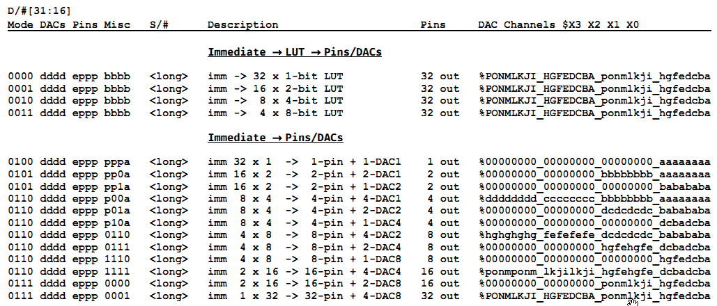
RDFAST modes only make sense for large block transfers. For single long transfers I'd use one of the immediate modes. I need no DAC so I set %dddd=0. If I understand it correct the modes X_IMM_8X4_4DAC1 to X_IMM_8X4_1DAC4 differ only in the way the bits are routed to the DACs. If I want to output 4 bits directly to pins or one nibble for each NCO rollover I can use any of them. %pppp specifies the base pin number. %e must be '1' to enable pin output. %a selects between LSN (bottom nibble) first for a=0 or MSN (top nibble) first for a=1.
There is no Pins -> immediate mode so I have to use Pins -> WRFAST to a dummy buffer in hub RAM and then RDLONG it later. Everything correct?
Yes, that's how it works. You have to fish the read value out of hub RAM when it's done. Theres a WAITXFI instruction for waiting on the command queue to run out. Also, take note that the immediate modes have no alternate order bit, they always send the lowest bit/nibble/byte/word first. There's a four-instruction sequence to reverse the nibbles that I use for PSRAMs (that need commands in MSB-first format).
Huh? According to the table the 8, 16 and 32 bit modes don't have an alternate bit. But the one to four bit modes do. Or are the docs wrong? Changing the nibble sequence should be a single REV instruction. We could swap the pin order on the PCB if required. For a RAM chip the bit sequence of address and data is arbitrary, anyway, only the commands matter. If you write in the wrong order you get it back in the same order, so no problem. In my case the bits of the registers of the LAN9252 have individual meanings so the bit order matters. But luckily the bit orders of commands, address and data are the same. Only the byte order is reversed for address and data. But that can be fixed with a single MOVBYTS instruction.
Today, I've tested SQI output with the streamer and it seems to work. It takes a lot less instructions than with 4 individual smart pins as the 4 data pins can be a continous group which can be setup with a single instruction using ADDPINS. However, the silicon is indeed wrong. The %a bit seems to have no effect at all in the immediate streamer modes.
I also decided to swap the nibbles with the correct bit order instead of reversing all bits and miror the four data lines on the PCB as this gives a more logical signal ordering.
CON _xtlfreq = 25_000_000 ' KISS board _clkfreq = 200_000_000 ' clock frequency 200MHz XCLKDIV = $2000_0000 ' streamer NCO = _clkfreq/4 = 50MHz cmdRead = $03 ' read with no dummy byte, 30MHz max cmdWrite = $02 ' write (SPI or SQI) cmdEqio = $38 ' switch to SQI cmdFRead = $0B ' fast read with dummy byte (SPI or SQI) modeSCLK = P_TRANSITION + P_OE + P_INVERT_OUTPUT modeMOSI = P_SYNC_TX + P_OE + P_MINUS1_B modeMISO = P_SYNC_RX + P_MINUS2_B modeSQIC = X_IMM_8X4_4DAC1 + X_PINS_ON + 6 ' streamer command TX 3 bytes = 6 nibbles modeSQIW = X_IMM_8X4_4DAC1 + X_PINS_ON + 8 ' streamer write, TX 4 bytes = 8 nibbles VAR long pinCS ' chip select long pinSCLK ' serial clock pin long pinMOSI ' SIO0 or MOSI long pinMISO ' SIO1 or MISO long pinsAll long modeCmd ' streamer mode command out PUB Start (pinBase) pinBase&= $3C ' 0,4,8...60 pinCS := pinBase + 2 pinSCLK:= pinBase + 3 pinMOSI:= pinBase + 4 ' SCLK + 1 pinMISO:= pinBase + 5 ' SCLK + 2 'pinSIO2:= pinBase + 6 'pinSIO3:= pinBase + 7 pinsAll:= pinMOSI ADDPINS 3 ' all data pins modeCmd:= modeSQIC | pinMOSI<<17 pinh (pinCS) wrpin (pinSCLK, modeSCLK) pinh (pinSCLK) PUB WriteSqi (regAdr, data) | cs, sclk, sio0, sio1, all, mode ' write one register via SQI longmove (@cs, @pinCS, 6) ORG movbyts regAdr,#%11_10_00_01 ' swap bytes, address is big-endian rolbyte regAdr,#cmdWrite,#0 ' command first mergeb regAdr rol regAdr,#16 ' swap nibbles splitb regAdr setxfrq ##XCLKDIV drvl all drvl cs wxpin #2,sclk ' syclk/4 xinit mode,regAdr ' start streamer wypin #28,sclk ' start clock mergeb data rol data,#16 ' swap nibbles splitb data add mode,#2 ' 8 instead of 6 nibbles xcont mode,data waitxfi dirl all drvh cs ENDThis isn't entirely true, because SQI RAMs are burst devices that will read multiple consecutive bytes from incrementing addresses. In theory the row addresses are arbitrary, but since only the bottom half of possible rows is actually present, the address needs to be correctly transformed, anyways.
Huh, I just noticed that the alternate bit is listed for these modes. I'd have remembered it being re-purposed, as in the immediate->LUT modes. How strange.
Chip has been careful with stuff like that. Every time I thought I found something wrong it was just me either not reading enough, misread/misunderstood it or I messed up with buggy code.
Well, the docs are either wrong, incomplete or misleading. I've checked both states of the a-bit and I'm pretty sure it has absolutely no effect on the order of bits that are output by the streamer to the pins. Maybe there is some misunderstanding and I expect something different from what Chip actually implemented. Maybe the alternate bit affects only the bits sent to the DACs which I do not use.
I'm not sure what this means. What is the "data sequence within the individual bytes"? In the 4-pin modes there are no bytes but nibbles. I would expect that a longword $12345678 is shifted out as nibbles with the $8 nibble first and $1 last in normal mode and $1 first and $8 last in alternate mode. But this is definitely not the case.
Alternate mode would do 7 8 5 6 3 4 1 2 then. Which would track with how the hub memory read/write modes work.
Ah, OK, that would explain why the 8, 16 and 32 pin modes do not have an alternate mode. Sometimes it's difficult to understand the meaning of an explanation if you don't know the intention of the creator. I'll check that out tomorrow.