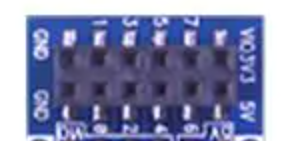
2x6 Connectors on Edge accessory boards
 ke4pjw
Posts: 1,321
in Propeller 2
Does anyone know where to source these connectors? Any suggestions on hole and pad sizes to allow pins to pass through?

Thanks,
Terry


Comments
Digikey 952-3211-ND
https://www.digikey.com/en/products/detail/harwin-inc/M20-7810645/6564947
If you use DipTrace I can send you a blank board project with that connector.
Thanks Jon! With knowing what to look for, I was able to find the symbol, footprint, and 3d model on Mouser's site. I am in the process of learning KiCad. I really appreciate it! Hopefully I will have a new accessory board to show off soon.
This group of boards I'm working on now is supposed to be my last before moving to KiCad. Lachlan recommended this book some time back (his friend wrote it):
-- https://www.amazon.com/gp/product/1907920749
It's been sitting on my desk longer that I want to admit. It's very hard moving to a new tool after so much investment in an old one....
Not strictly my friend - though I'd happily befriend him if I ever ran into him, because he does good things like that book. He's in Sydney, i believe. But yes, that book useful for moving past a few sticking points and gaining confidence in general. Its the next best thing after this forum.
Brian and I have been using Kicad a bit recently. Kicad version 7 was recently released and has some nifty features like attempting to complete track routing to its target destination, command line control, negative text etc
That's the part I'm using too, M20-7810645.
I think the Parallax part is different. Think I found part # for it once, but not available at Digikey or Mouser...
In Eagle, was able to connect pads to vias so can use vias for routing, like Parallax does. Also, made the via rings thin, so can better route wires between them...
Have to be careful not to run traces over the holes...
Oh, I got that part number from Ken Gracey. Even if it is different, I know it works because I've built boards with it.
DipTrace has a feature where you can have two pads in a partern with the same number (using @), so even though I have 24 pads (12 smd, 12 t/h), the component (to the rest of the DipTrace ecosystem) only has 12 pads.
Wait, don't all of you down under know each other?
Jokes aside, it is a good book that I purchased for myself and a colleague. Now I have put it to use! I just installed version 7 last night.
I will pick it up. Looks good. Thanks!
I really wished I took the time last August to do my last board layout in KiCad. I upgraded from ExpressPCB to ExpressPCBPlus. The "Plus" was it being a pain the butt, I think. I am sure there are some niceties that their software brings, that masks issues that may crop up going to fabrication. Being locked into their fab first, before being able to get gerbers is my main motivation to move away.
The fact you can render pretty 3d models in KiCad is what drew me to it. So far, following the process used in the 20 minute tutorial I found on Youtube, KiCad has been a dream. The only thing I have found to be a pain was figuring out how to associate the component footprint with the models I downloaded from Mouser. Once I figured out the secret handshake it has worked out well.
What Jon and Rayman are reporting is all spot-on.
That M20 part was used originally. After a while it became difficult to source and at least one alternative was used. It's possible that the M20 is now back in use sometimes. Or not.
Anything with the same specs will be fine- there's a few compatible versions of those connectors from different manufacturers.
If the locating lugs make routing an issue, then you might consider snipping off the locating lugs, or buying a version of the socket without them. Hand-soldered boards don't need those lugs- they are only to prevent the connectors rotating in the oven for automated builds.
Or use a standard 0.1" 2x6 through-hole socket. A couple of the Parallax add-ons used those where mfg was an issue, or the board purposefully needed raising up a little.
Eagle is strange in many ways... even though I connected the via and the pad in the library and they overlap, still have to draw wire between via and pad to get rid of airwires...
BTW: Other thing to watch out for is that your board doesn't interfere with the ground lug between the connectors...
How far apart are the dual connectors? I measured almost 41mm, outside to outside of the pins with my calipers.
They are on 1.1" apart centres
For what you're measuring you should see 1.6" (pin to pin centres) + 0.025" gold pin thickness, or 41.275mm
I agree with Lachlan. From my P1 Dev board (like an Eval board for the FLiP)
If you're doing a lot of measuring (I do), treat yourself to an inexpensive set of electronic calipers (~$35 on Amazon). In this situation you can measure the thickness of a pin, and while on the pin reset the caliper to 0. When you measure from the outside of two pins, you'll have the pin-to-pin distance. Don't forget to close the jaws and reset your zero before you measure something else!
If the GND terminal were removed a standard 34-way ribbon cable could be attached to both headers.
Thanks all! I think I got it! This is my first SMT board. Definitely more challenging than through hole to lay out.