

SMPS Smart pin mode
 n_ermosh
Posts: 303
n_ermosh
Posts: 303
Has anyone built any switching power supplies with the smart pin mode? I need to build a 10A switching supply and parts are hard to get right now, only option is to buy the $10 LT parts and I don't want to do that if I already have a P2 on board that could do it instead ![]() , but only if I can do it without software interaction.
, but only if I can do it without software interaction.
Reading the docs and other forum posts (1, 2, 3), and I'm a bit confused about how the smart pin mode is intended to work. How I understand it now is that it's a simple sawtooth PWM modes with 2 enables (one synchronous, one async). However, you can link the sync input (the A input) to another DAC compare smart pin, and use that as the voltage feedback input. This sounds like I should be able to run a simple switcher completely with smart pins and no CPU interaction. Is that correct? If so, it raises the following questions:
- Whats the point of the PWM? Shouldn't that just be set the output high, and then output low whenever the A input is high.
- The above can be done with other smart pin modes, right? Something like output high when the level compare outputs low and output low when the level compare is high, using a clocked compare pin to set the switching frequency.
- Is the idea there should be multiple PWM cycles to charge up the LC tank before it is shutdown while the load discharges the LC tank?
- The docs mention that Y can be set once and run indefinitely. How would you go about selecting a PWM value to use, since the output voltage is also being set by an external divider and the DAC level in the adjacent comparator.
- The line in the docs "After 'A' reads low, Y[15:0] is captured, IN is raised, and the process repeats.", implies that the PWM cycle is automatically restarted when A is low and Y is read in again? or will it continue to the end of the PWM frame and continue running as is?
- Or, am I just overthinking this, and all these features are just to create a flexible structure, and there are just multiple ways to skin a cat?
Comments
What topology of power supply are you looking for? And input, output voltage? I'll assume a buck converter for the rest of the discussion. For 10a current that means a synchronous buck converter.
I've build one using the P2 and it can do close to 10A. I use 2 cogs. 1 for ADC measurement and PID controller. 1 dedicated to PWM. I don't use the PWM smart pin mode because I add a programmed dead time between the high side and low side outputs. To have both mosfets on at the same time would be catastrophic. The good thing is a synchronous buck converter runs at a nearly fixed duty cycle dictated by the ratio of input to output voltage.
The PWM needs to switch off periodically even if the voltage is below the setpoint to limit current through the inductor and mosfet. A higher switching frequency allows a smaller inductor value.
It's not realistic to charge the output capacitors in 1 PWM period or even tens of PWM periods.
A synchronous buck converter can't just output low when the output voltage is reached. That would cause it to discharge the output at a high current.
I'm not exactly convinced the SMPS mode will regulate voltage well. It seems ideal for a hardware current limit though.
I've heard that the comparator is not that fast. It would need operate over several P2 clock cycles to actually control the PWM effectively. Otherwise it is replacing a PID controller with a bang-bang controller in a situation where tuning the PID controller was hard enough.
Thanks for the input. Yes, you are correct, I was thinking about a buck converter. I’m hoping to avoid having to do a synchronous one with a beefy diode instead, but that might not be possible and I’d be wasting my time. I should mention my 10A requirement is peak, not continuous. Like 3A continuous. Even if I have to go synchronous, maybe I can add the dead time circuitry in hardware instead of software, since I’d need a gate driver anyway.
I was hoping the SMPS mode was a nice and ready to go mode to do voltage control, but if it requires constant software attention probably not worth it anymore. I’ll lay it out and try it, even if just to experiment.
In any case, I’m still a bit lost with what the A input actually does and how it controls the PWM output. Seems like PWM duty cycle is fixed by Y, in which case you need to add a software controller to actually regulate and then it basically becomes the design you described.
I suspect the comparator is fast enough, just its slow-DAC set-point takes some time to settle.
Using a whole P2 just to control a single SMPS is somewhat overkill and too expensive. The SMPS smart pin mode might be useful if you need the P2 anyway, say you have a BLDC motor controller and want to add a PFC or a buck or boost converter to fit a battery pack with too much or too little cells.
As gate driver check out the EG2104. It's the Chinese version if the IR2104 but has
The "M" version is similar to the original IR2104. The "S" version has more drive strength and ~500ns dead time (good for slower IGBTs). The version without suffix has ~100ns dead time which is ideal for fast switching, synchronous MOSFET converters.
I will have a P2 on this board regardless, so I’m not adding cost by trying to use it as a supply controller, and in almost any situation it would be overkill, but given how unpredictable component supply is nowadays, it doesn’t feel like such a crazy idea…
The latest P2 silicon documentation has more info about the SMPS mode. https://docs.google.com/document/d/1gn6oaT5Ib7CytvlZHacmrSbVBJsD9t_-kmvjd7nUR6o/edit#heading=h.nb3tj4pl85da
Is there a reason why you don't want a software controlled power supply?
Also, what will the minimum load be? Light loads will force a non-synchronous converter into discontinuous mode. The output voltage will rise unless the duty cycle is reduced significantly. https://en.wikipedia.org/wiki/Buck_converter#From_discontinuous_to_continuous_mode_(and_vice_versa)
Mainly, don’t want to use 1-2 cogs for it, and don’t want to mess with tuning digital software loops. For this project I could get away with this, but I have another project coming up where I need to build a power distribution system and have 16 controllable supplies on a board (fixed voltage, but they each need enable/disable and overcurrent protection. But they are smaller, 5V, 2A each). So if could use a P2 as a controller for all those supplies, that would be pretty cool.
Anyway, for this one, minimum load will be light, 100mA maybe, so it’s very likely to require a discontinuous mode anyway.
I found a cool and cheap gate driver I can use to make it a synchronous design without extra effort. Built in dead time is set with an external resistor and it has wide supply range. Most importantly, very well stocked")
Could you please post a complete list of your requirements? Then I could possibly come up with an idea how I would do it.
The list is below, but before getting into the weeds of designing that system, I do want to understand how the smart pin mode actually works, even if just for my own education. That docs are not clear enough, and my experimentation hasn’t really yielded much. From what I understand, it’s simply a pwm pin with two enabled/disable inputs. Is that correct? Or does the A pin do something more than just enable/disable pwm on every frame rollover?
For my power distribution project. It’s not fully thought out yet but here’s what I can think of:
My idea was to us 5 pins per supply: 1 SMPS smart pin, 1 DAC compare for the A input of the smart pin, 1 DAC compare for the B input of the smart pin, 1 ADC for voltage measurement, and 1 ADC for current measurement. I want do a dynamic overcurrent protection, that takes the time the current is high into account (very short pulses pass through, but sustained OC gets turned off, that sort of thing). With my other pin constraints, I have 32 pins free, so I can do 5 supplies. I was thinking of just adding a second dedicated p2 to then do the others, and I like that way because then the design is scalable in case I find I need more than 16 supplies. The main p2 would handle the off-board comms, then it would have peripheral P2s for supply control.
Did Chip ever do a published example of SMPS-PWM mode ?
I did find this
https://forums.parallax.com/discussion/174284/p2-smart-pin-drive-class-e-amplifier
and from what I recall of the discussions the PWM block had two control inputs, for I and V, usually via DAC+comparator threshold settings (as in post #7).
I control is simplest, a direct cycle by cycle trip.
Did you get PWM control via SW [Y] and trip via B operating ok ? (static A?)
The A control seems the poorest documented.
I also find this
https://forums.parallax.com/discussion/172879/smart-pin-example-pwm-switch-mode-power-supply
Chip says:
In a buck converter, that B sense would usually be current from the upper FET, via a current sense amplifier.
The A pin here is more over-voltage/PWM enable, rather than control, but could be ok for cap-charging type uses. (burst of pulses then cease)
SMPS converters in light load mode also work 'gated' like this, but at full load, separate control of PWM duty is needed.
FWIR there was discussion around a simple Up/Dn counter PWM control - that needs SW, but not very much, and one COG could manage many SPMS cellls.
Up/Dn concept :
Where a slow counter ramps PWM, one click at a time, in a form of soft start, and then when voltage threshold is reached, a FB pin changes slow-count direction.
That means the pwm would ramp, then continually jitter around the control point, unless a step load change occurs.
Step Load decrease would see a output bump, and then PWM setpoint DEC's the few counts until the FB-feedback jitter resumes.
Step load increase, would see a output droop, and PWM setpoint INCs the few counts until the FB-feedback jitter resumes.
Slow counter sets the response rate, and is not suited to discontinuous control, so full sync power stage is needed.
That manages light loads, at reduced efficiency.
The FET+inductor resistances set the 'stiffness', so you would usually choose those conservatively (tho most already do that for lowest heating)
A challenge becomes could you use a single Pin for both over-voltage/PWM enable, and PWM duty control ?
Maybe that could work, in a buck design where A! is HW/Enable sampled at PWM end, and it could be SW sampled at PWM mid, for control.
The natural triangle ripple would mean A starts pulsing low at ripple peak, and as voltage increases, A 'spreads' to become 100% low.
Possibly A may need SW sampling at two points, to avoid light loads pushing the control loop far one way.
Call these Ap and Ae : - normal feedback control is Ap = L and Ae = Hi, and Enable control is Ap = L & Ae = L and ramp up / soft start is Ap = H and Ae = H
When in Enable control/burst mode, the PWM would be set for best guess (or last control value) and some Sw could measure Vin and use expected Vo to limit the PWM max.
addit: Some careful RC filtering could be needed on the A sense to remove the switching spikes that are always there in SMPS. You want to remove the unwanted spikes, but keep the useful mV triangle wave.
What output voltages ?
With that many SMPS, if the loads are similar, you can start to interleave the phases to reduce the ripple peaks on the input side.
The P2 launches each PWM with a slight delay, and then checks the A control info mentioned above, in a similar delay fashion. 1 COG could manage 16 SMPS.
Right, forgot to mention output voltage--adjustable 5-12V (software should set the value), and lets say 50mVpp output ripple.
I've read through those forum posts, and they don't seem to describe the A function well either. I experimented by setting up a pot connected to the A input and set the DAC level to 50%. I swept the pot and looked at the pwm output on from the smart pin, and it would just pulse PWM that I set when A is low, and keep the output low when A is high (might have gotten high/low reversed, don't remember what the polarity was). However, if PWM is set to 100%, output never goes low. I will set up another test that will step the DAC input mid PWM cycle to see what happens.
Overall, it seems this just a PWM mode that has 2 control pins, rather than a simple 2 input logic pin.
The up/down idea is interesting, though it feels reminiscent of a crude I controller. And making it a PI could then keep the voltage steady rather than oscillating around the set point in a triangle fashion for not much more effort. I think I'll get a board made with a FET/driver/inductor/cap loop on it and play with different ideas. The alternate sampling of voltage/current is an interesting idea too. I'd bet there's a way to do full control of an output channel with just 2 pins, just requires some creativity.
That confirms the over-voltage/PWM enable type action (ie just go/no go) that Chip described.
Ideally, it would not fail at 100%, but that oops/bug is likely an artifact of the way 100% is handled, and in practical uses, you would not run 100% PWM in SMPS.
SW can avoid that 100% setting too.
Keep in mind the LSB of PWM will be quite small, as a % of full scale.
In the simplest form a +/-1 U/D counter may have poorer step responses, tho a 'stiff' power block means less dT for a given dV.
SW could create an adaptive counter, that increases the delta when many are all the same way, and reduces the delta once it starts toggling.
You might be able to combine the DAC-Compare pin with ADC in, so you can drop it to 3 pins from 5 ie Is, Vs and PWM_out
I'm not sure how well ADC tracks the pin threshold DAC, in an ideal system you could set the DAC+Comp trip point, just above the normal ADC control point.
Ok, 1..2A should be possible with a single high side MOSFET switch and a low side flywheel shottky diode per channel so you don't need to worry about dead time and shot-through. But with the wide input voltage range, the adjustable output voltages and the wide min:max current rating (50mA:2A) you'll need a fully closed PID control loop. So I think you need at least 3 pins per channel.
So you can do up to 10 channeld with 32 pins.
so here's the design I came up with:
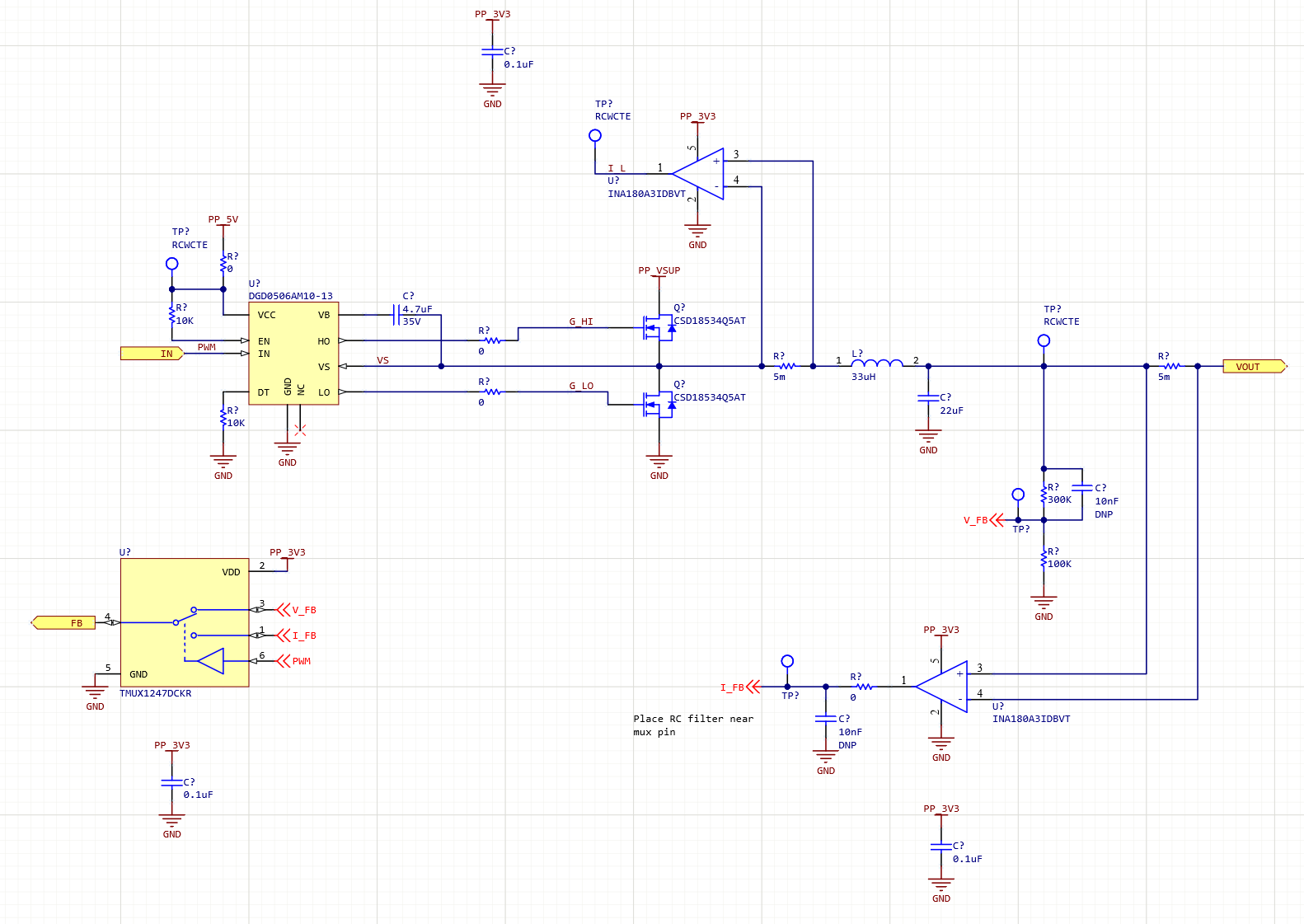
I would need a fet gate driver no matter what, so I figured I'd just go with a synchronous design. The driver IC handles the dead time and shoot through issues, so I don't need to worry about that. The two feedbacks are put through a mux controlled by the PWM signal. This will make is so that the current is sampled after the rising edge of the PWM, and voltage on the falling edge. as a result, there will be a minimum and maximum duty cycle to make sure each signal is present long enough, which will likely limit the switching frequency to around 100-200khz, depending the ADC sampling period I go with, but I can probably got with 6 or 7 bits, since I don't need a ton of resolution here. For light loads, I can just stretch the frequency to lower the duty cycle but maintain a minimum on time. I also don't need the current to be sampled every cycle, I can stretch it out over multiple cycles and accumulate it to increase resolution
For output enable/disable, I'm thinking to just put an ideal diode circuit at the output (which will also protect against backdriving this supply), and when I want to disable the output, just drive the PWM to 0 so output of the converter is 0, and diode makes the output float.
For the actual timing, if I go with 7 bits, I can do 64 clocks to get a sample, and if I limit that to 5% duty cycle minimum, then that comes out to a max frequency of about 230khz at 300MHz system clock (which is what I've been running all my boards at). I just need to be smart about when the cycle I switch the adc to sample vio/gio.
I'll need to actually measure up all the propagation delays and figure out the overall loop delay to know what bandwidth I can get out of this, but I'm hoping I can get 20kHz-30kHz without much tuning effort.
Some gate drivers support a 3rd state, which turns off both output FETS when the drive-in pin is floated.
Otherwise you can use the EN pin, as you will need something that manages the time when P2 is in reset and booting. (pins floating)
Sounds tricky, it might be easiest to initially test things with separate I and V ADC's, then see if you can time-share them later.
Doesn't look like this driver has that feature, but if I just leave the EN tied high and add the ideal diode to the output, it solves both issues and the output is only enabled when the P2 is powered and actively driving PWM.
Yeah I added pads on the board to bypass the mux with 0ohm jumpers so I can try out both options
Maybe choose one that does have the feature ? eg NCP81151B etc
That 3-mode feature allows P2 to SW change between low-power diode-flyback mode and full sync drive, on the fly, and importantly auto-protects during P2 reset.
Adding an ideal diode, means you need to check/hope the SMPS output cap is at a known safe voltage.
thanks for the suggestion--I'm planning to put two converters on my test board, I'll try that driver on one of them.
Can you clarify why this is the case? the output cap can't ever be charged above the input supply voltage (30V in my case), and I can put a bleed resistor to keep it discharged (something like a 10k will do fine) when the system is off/booting. As long as the ideal diode is rated to well above that, should always be safe, right?
It means you need to include time for that bleed to work, and you have no low power idle mode.")
For development anyway, I'd include an ideal-diode, and then see if it really is necessary. Always easier to remove it, than add it later
I'd recommend the inductor current sense resistor go between the inductor and capacitor. That will reduce the common-mode voltage that the amplifer must filter.
A lot of gate drivers have separate high and low side input. With these, the tri-state output is easy and automatic when the P2 is not operating. The downside is the P2 must generate the deadtime. Maybe the streamer could be used to drive a bunch of PWMs at once.
The issue with tying the enable pin high is that when you reset the P2, the low side fet will stay on and rapidly discharge the capacitor. I think it would be fine to have one global enable pin for all of the converters. I don't expect an ideal diode to operate at 100kHz. If it did work then I think that would make things operate like a non-synchronous converter. After the capacitor would be fine.
If you measure the input voltage as well as the output capacitor voltage you can calculate the duty cycle required to start a buck converter without a current transient. Very important for a battery charger where the capacitors are charged at startup.
https://www.realsolarcars.com/assets/sce.zip
There are parts like this
https://www.diodes.com/part/view/APR34910/
from this series
https://www.diodes.com/products/power-management/ac-dc-converters/synchronous-rectification-switcher-and-controller/
that are designed as lower-loss flyback ideal diodes, in SMPS.
APR34910 is an interesting part as it includes a 10 mOhm 100V fet plus the gate drive for flyback diode emulation.
I think the OP is trying to reduce parts source risks, so they may prefer multi sourced parts ?
I'm happy to be wrong about that. What a nice surprise!
Exactly.
For now, I just want to prove the actual converter concept. I'll worry about protection and all that later once I'm building an actual design. I'll get boards on order today and let you know if it ends up working.
I'd suggest adding an ADC path to the SMPS Supply voltage, and a DAC + resistor path to the feedback setpoint, to give more trim choices.