

Weird SPI Transmit Bug; clock is shifted by 1 bit - Spin 2
 Nicopowers
Posts: 12
Nicopowers
Posts: 12
Hello Parallax Forum,
I am learning how to use Smart Pins so I decided to make my own SPI driver; for now I am only trying to transmit data, and it is almost working but for some reason the clock is starting too late it seems. I am trying to transmit $34 but it is really sending out $1A; which is $34 shifted to the right 1 bit, so the SPI clock is offset by 1 cycle (so it seems).
I tried to make my code as easy as possible to understand for me, I know JonnyMac has some Spin 2 code on Github, but I had trouble understanding it so I wanted to take a simpler approach for now, and I am trying to get more familiar with Spin 2 and PASM. Here is my code:
PUB main()

' setup SPI CLK
disableSmartPin(spi_clk)
WRPIN(spi_clk, P_OE | P_TRANSITION)
WXPIN(spi_clk, 100000)
enableSmartPin(spi_clk)

' setup SPI MOSI
disableSmartPin(spi_mosi)
WRPIN(spi_mosi, P_MINUS1_B | P_OE | P_SYNC_TX)
WXPIN(spi_mosi, $27) ' x[5] = 1 for start-stop mode, x[4:0] = 7 for 8-bit data, so $27 = 0010_0111 in binary
enableSmartPin(spi_mosi)

' start data transmission

' pull CS low
pinl(spi_cs)

' fill data buffer
WYPIN(spi_mosi, $34)
' start clocking out data
WYPIN(spi_clk, 16)
' wait for data to be sent
waitForIN(spi_clk)


disableSmartPin(spi_mosi)
disableSmartPin(spi_clk)


' pull CS high
pinh(spi_cs)

' wait forever, code is done
repeat
Where waitForIN is just polling the IN bit until it is set, and then clears it by acknowledging it:
PUB waitForIN(pin)

org

WAIT_IN
testp pin wc                    ' get state of IN bit for smart pin, store in C
wrc pr0                         ' store C in PR0 to perform conditional branch
tjnz pr0, #IN_SET               ' if C is set (IN = 1), branch to IN_SET
jmp #WAIT_IN                    ' if C is NOT set, go back to WAIT_IN to continue polling

IN_SET
akpin pin                       ' ack IN to clear it
debug("in set")

end
And enabling and disabling the smart pins just changes the DIR for each pin:
PRI disableSmartPin(pin)

org
dirl pin
end


PRI enableSmartPin(pin)

org
dirh pin
end
This is what the logic analyzer waveforms looks like: 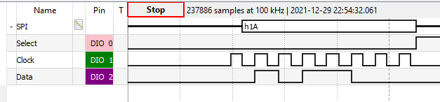
As you can see, the clock looks as if it is starting too late, if it started 1 period sooner, it would have got the right data.
Is there an optional config parameter I am missing when I setup the X registers for the spi_clk or spi_mosi pins? I don't know what I could be doing wrong.
Thank you!
Nick
Comments
So I fixed it by shifting the data I want to send by 1 bit to the left, but why do I have to do this?
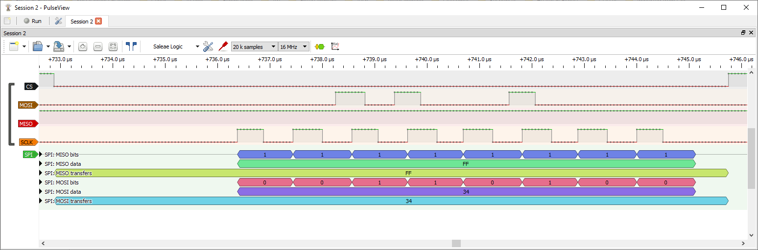
WYPIN(spi_mosi, ($34 << 1)) --> works, ouputs $34WYPIN(spi_mosi, $34) --> does NOT works, ouputs $1AIt's not a problem with your Smart Pins -- it's an error with your logic analyzer (my cheap one does the same thing, so I've got a proper Saleae on the way).
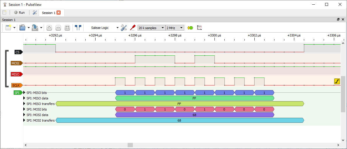
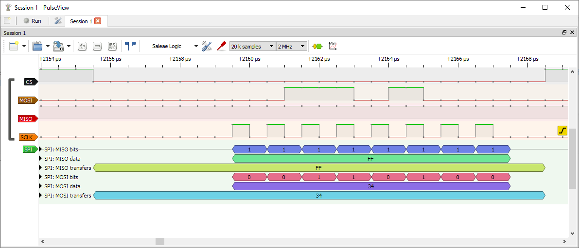
What's happening? The P2 Smart Pin doesn't know the SCLK frequency, so the MOSI transitions for the next bit within a couple ticks of the rising edge of the SCLK output. With sampling/quantization in the LA hardware and firmware, you can get misreads with Smart Pins. My case is the opposite of yours: my cheap LA says $68 when it should be $34. Playing with LA sample size and timing, I could sometimes get the correct reading, but it was never consistent.
If your requirement is as simple as you indicate, switch to inline PASM. In this extremely simple code (which runs at about 1MHz), the rising edge of the clock is delayed 1/4 clock period which ensures the MOSI output is settled/registered before the clock goes high.
pub shiftout(value) | t

  t := ((clkfreq / 1_000_000) >> 2) - 3                         ' ~1MHz SPI clock

  org
                ror       value, #8                             ' move msb to bit31

                rep       #9, #8                                ' 9 instructions run 8x
                 shl      value, #1                     wc      ' get msb from value
                 drvc     #MOSI                                 ' write to mosi
                 waitx    t                                     ' let mosi settle
                 drvh     #SCLK                                 ' clock it
                 waitx    t                                     ' finish bit
                 drvl     #MOSI
                 waitx    t
                 drvl     #SCLK
                 waitx    t
  end
The setup for this code is really easy:
Smart Pins are a solution, but not always the best solution. As you can plainly see, this code is significantly simpler than when using Smart Pins. There's actually less of it, too.
Here's the capture of the inline PASM2 version from my super cheap ($13) logic analyzer:
Note that calculating t every time adds a delay between CS dropping and the first bit. In practice, I would make t a constant as with the SPI IO pins. This code also takes MOSI low at the end of each half-bit period. This makes individual bits easier to view, and leaves MOSI in a known state (low) on exit.
BTW: You need to use pinfloat() to disable/reset a smart pin if you continue down that road. It's the DIR bit in the pin that counts, not the OUT state.
You might want to invert the B input on your TX pin, this way the data would change on the negative edge and it's ensured that it is stable when the positive clock edge comes. Make sure to give the Data smartpin a start ahead to get the first bit right (you could invert the clock output itself so it will start with a 0, meanwhile the Data pin will put it's bit #31 on the line).
That works better than I expected. Here is the non-inverted trace:
And here is the output with the B pin into the SPI TX inverted. Note that the 1st high bit on MISO is no after the second falling edge of the clock.
The result of the inversion is to delay the new MISO output by half a bit period -- this gives the SPI decoder space to see MISO before the clock bit goes high.
As a test, I added this to my SP SPI flash object -- everything seems to work okay with the inversion.
It's important to remember that this is solving a problem for the logic analyzer that is not a problem for SPI hardware.
Please note that there is in each SPI device manufacturer's datasheet a section that defines for how long a valid signal must be on the Data input before the clock ticks and for how long it shall stay stable after the positive clock edge. so to make it 100% bulletproof you would stick to these specifications. it's convenient to just change the Data pin on the opposite clock edge so the requirements are met without much consideration.
reading is of course the opposite, always exactly on the positive edge
some protocols are oriented upon a negative clock edge, in these cases everything is the other way around of course
I think these diagrams illustrate what's happening. With a typical setup, the SPI TX pin outputs a bit immediately after this code:
We can load, start, and wait for the clock to finish with this:
The resultant output is:
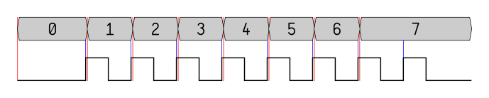
Note how close the LA sample (rising edge [blue]) is to the P2 Smart Pin setting up the next bit (red) -- the new bit is output two internal clock cycles after the rising edge of SCLK. I believe both events are getting caught in the same sample period of the LA which is causing a misinterpretation of the signals.
If we put a virtual inverter between the clock signal and the SP SPI engine with this setup (note P_INVERT_B [SCLK]):
...the net effect is that we delay the setup of the next bit by half a clock period which allows the LA bit sample and the SP bit change to happen in different samples.
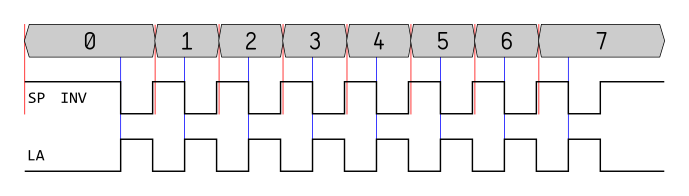
Keep in mind that by using P_INVERT_B you art not changing the external SCLK signal, just how the SP logic sees SCLK.
Here are the two methods used in testing