

Where can I see a detailed description of a register?
 Nicopowers
Posts: 12
Nicopowers
Posts: 12
Hello,
If I wish to view a detailed look at the register contents say, for example, OUTA; where can I see this information?
I couldn't find a document that offers a register view that shows what each bit represents. I am looking for something similar to this:
I ask this because I know OUTA/B is supposed to be a 32 bit register, but for some reason when I try compiling spin 2 code to modify the register with a 32-bit value, it says its contents can only be 0 to 511? But that range would represent a 9 bit register, and 2^32 is 4,294,967,296, so shouldn't OUTA and all other 32-bit registers go to 0 to 4,294,967,295 in decimal value?
This is the error I am getting: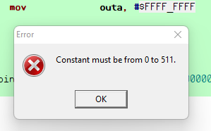
Thanks!
Comments
The original 8080, 8085, 80186, Z80 processors used registers for athematic operations and for stack pointer and program counter.
The P1/P2 are more like mainframe computers that used memory mapped registers that can be accessed by knowing their memory location.
Since there are multiple COGs there are multiple registers:
COG REGISTER LAYOUT
The cog's 512 x 32 dual-port RAM, used for code and data, is mapped as follows:
$000..$1EF RAM general-use code/data registers
$1F0 RAM / IJMP3 interrupt call address for INT3
$1F1 RAM / IRET3 interrupt return address for INT3
$1F2 RAM / IJMP2 interrupt call address for INT2
$1F3 RAM / IRET2 interrupt return address for INT2
$1F4 RAM / IJMP1 interrupt call address for INT1
$1F5 RAM / IRET1 interrupt return address for INT1
$1F6 RAM / PA CALLD-imm return, CALLPA parameter, or LOC address
$1F7 RAM / PB CALLD-imm return, CALLPB parameter, or LOC address
$1F8 PTRA pointer A to hub RAM
$1F9 PTRB pointer B to hub RAM
$1FA DIRA output enables for P31..P0
$1FB DIRB output enables for P63..P32
$1FC OUTA output states for P31..P0
$1FD OUTB output states for P63..P32
$1FE INA * input states for P31..P0
$1FF INB ** input states for P63..P32
Mike
Hello Mike,
Thanks for the info, so yes for OUTA and OUTB, for instance, it says it controls the output states for P31 to P0, so then I would assume that it should have 32 bits; where each bit represents a pin, right? But how come I can only mov a value of up to 9 bits in OUTA and OUTB when it should be a 32 bit register?
The source field of most of the instructions is 9 bits. This can contain either a register address (0 to 511) or a constant (9 bits). If it's a constant, you have to preceed it with a "#" so the assembler can set the instruction bit that tells the hardware that the source field contains a 9-bit constant rather than an address (like OUTA or OUTB). The default assumption is that the source field is a register address.
Ohhh ok, so basically if I want to write a 32-bit value to a register, I can't simply move an immediate 32-bit value into a register? I need to move another register that contains the 32-bit value that I want, into the destination register, in this case OUTA?
But if this is the case, how would I ever be able to write a 32-bit value into a register to get this started? Will I need to use PTRA or PTRB that points to a 32-bit value I wish to move into OUTA or OUTB?
Thanks!
If you use the P2, you can simply write:
This compiles to 2 instructions, an AUGS that provides the top 23 bits, and the MOV with the lower 9 bits. You just can not encode a 32 bits immediate value in a 32bit instruction word.
On the P1 you need to preload a register with the 32bit value and access that.
Andy
Oh wow that's an interesting directive. Thanks! Yea I figured out another way to do it like this too:
dat
        org   0

        dirh            #56 ADDPINS 1
        mov             outb, value_to_store

value_to_store          long    $0000_0000
What does AUGS stand for? And what does it mean to provide the top 23 bits and the MOV the lower 9 bits; the top 23 bits of what? And the lower 9 bits of what? The data? I see that would add up to 32 bits, but I don't see how that works exactly...
Also did you mean to say that you can not encode a 32-bit immediate value into a 9-bit instruction? Because that's what I was trying to do effectively. I didn't realize that was the address of the source.
Thanks!
Check the instruction encoding. The Propeller chips are RISC architectures, so all instructions are 32 bit and mostly share a common bit layout.
The D and S fields in each instruction are only 9 bits in size, which is enough to address any location in Cog RAM or give an immediate value 0..511. If you need a larger constant, you can either place it into a register or use AUGS/AUGD, which is a separate instruction with a special encoding that contains 23 bits, which are combined with the 9 bit immediate of the next instruction that has one in that slot (D for AUGD, S for AUGS) to make a full 32 bit immediate. Note that AUGx consumes 2 cycles like a regular instruction, so hoisting the value into a register makes sense for performance sensitive code.
Exceptions to the immediate rule are the load/store instructions, which without AUGS can only have immediate addresses in the range 0..255 (encoding space is used for PTRx-relative addressing modes) and some branches (JMP, CALL, CALLA, CALLB, CALLD and also LOC (which isn't a branch)), which always encode a 20 bit immediate.
On the bit layout of registers: All the ones that need it have a bit usage table description in the documentation. INx/OUTx/DIRx don't because they're just homogeneous I/O ports. Yes, the P2 documentation has a problem where it assumes some level of familiarity with P1.