

SINCx filtering: How many samples do you need?
 Rayman
Posts: 16,460
Rayman
Posts: 16,460
I just recently tried out the Smart Pin ADC modes and have a question...
First, here's my understanding of P2 ADC:
There is SINC2 sampling, which is straightforward, you just set it up and then read values. IMHO, there's no actual reason to mention SINC2 here, since it's baked into the hardware and it's probably how other chips work.
Then, there are these SINC2 and SINC3 filtering modes. These are more complicated and add an extra layer of filtering on top of the sampling. Docs say SINC2 is better for DC and SINC3 better for time varying signals. For these, you need to monitor INA and grab the value each time it goes high. Looks like you need to accumulate all these values to form the actual result. I believe @evanh is pointing out there is some complexity here as the results you get are 27-bit and you need to shift or treat carefully when doing 32-bit accumulation.
If I have this all right, my question is how many times do you need to sample and accumulate SINCx filtered values before you have an answer that gives the ENOB stated in the docs?
Comments
For SINC2, you'll get meaningful samples starting with the 2nd sample.
For SINC3, you'll get meaningful samples starting with the 3rd sample.
Thanks. I was thinking it would be many to get the ENOB stated.
One more question... Do you have to capture every sample, starting from the first one for this to work?
I'm thinking yes...
Sound like the first sample is a baseline and then the following samples are adjustments to add in.
Yes. Although the very first data word RDPIN provides can be a partial period due to switching between analogue sources ... or much more for frontend sigma-delta startup. The sigma-delta circuit is only running when selected in the pin config bits of WRPIN. Otherwise it is dormant. I think it's 100 microsecond warm up time that Chip allows.
Yes. They are deltas on deltas even, like acceleration.
Rayman,
The Sinc2 Sample mode is like this:
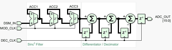
That diagram is for a Sinc3, hence it has three stages of each, accumulators and differentiators. So a Sinc2 is two of each instead. That's the "Sample" mode. And as you've guessed, most other sigma-delta ADCs will be doing the same.
What's different with the "Filter" modes is they are missing the differentiator stages. Well, the first differentiator is present in hardware through a freebie optimisation that Tony figured out. The missing differentiator stages are left for the software to handle. So that's why there is alway the SUB and ADD instruction pairs in the example uses.
I have to add some comments on ENOB... Please excuse me if my explanations are a bit fuzzy. I have to admit that I do not understand all of the "magic" of sigma delta ADC theory. But I think a fuzzy explanation that everybody understands is better than a true scientific one that almost nobody does. Please correct me if i'm wrong.
"Straight" sampling (mode %00, called SINC2 sampling in the data sheet) is simply summing up all 1 bits in the input stream over the sampling period. It has no (additional) delay so after the first period you have a valid result. The drawback is that here is always some oscillation at the RC summing point. This results in a fair amount of quantisation noise caused by randomly cutting off groups of 1s or 0s at the beginning and end of the sampling period. All bits are weighted equally. The theoretical ENOB is log2(# of clocks), the practical a bit less due to cut-off noise.
SINC2 filtering (mode %01) adds an integrator/differentiator. This effectively means that the window through which the input bitstream is looked at gets twice as wide and the bits are no longer weighted equally. Instead, a trapezoidal weighting mask is applied what results in a "fade-in" and "fade-out" at the window boundaries. That reduces the noise. The wider window adds one bit to the ENOB so we get log2(# of clocks per period)+1. The drawback is the delay. We get valid results only after the 2nd sample.
SINC3 filtering (mode %10) adds another integrator/differentiator stage. This means we have to wait for the 3rd sample for a valid result. The weighting function becomes parabola-shaped (similar to the "Tukey"-curve in the scope-mode ADC chapter). Noise is reduced further and ENOB becomes even better. The data sheet states log2(#clocks) * 2 which is twice as much compared to straight sampling! How does that work? The answer is, it doesn't, at least not in a perfect mathematical precise and guaranteed way. It works in a more "statistical" way. You might think that 3 * 256 = 768 bits do not contain enough information to get 16 ENOBs. That's true for a simple averaging.
But an SAR ADC (successive approximation) can extract 16 ENOBs out of only 16 sampled bits. The key is "modulation", or in other words cleverly applying different offesets to the comperator and weighting the resulting bits in a logarithmic way. This is the best possible modulation sheme and the maximum possible amount of information per bit with a single comperator. Equally weighted averaging is the worst method (that still makes sense) and requires 2^n sample bits for n ENOBs.
Sigma delta ADCs with SINC2 filtering are somewhere in between. A more or less uncontrolled oscillation plus some random noise is used for modulation. The ENOB stated in the data sheets are theoretical values. From my experience you can expect something like 12 truely usable bits with a sample period of 256 clocks and SINC3 filtering.
Thanks @evanh & @ManAtWork & @cgracey . I think I have a handle on this now.
I'm going to work on code that just does 2 samples for SINC2 filtering or 3 samples for SINC3 filtering and returns a value. The infinite loop example doesn't work for what I'm doing right now.
I just saw a comment by @cgracey in another thread that one needs 3 samples when in SINC2 filter mode if you change input source.
Think I'll just take 3 samples in SINC2 mode and 4 samples in SINC3 mode, just to be safe.
You're describing Sinc1 there, not Sinc2. The "Sampling" mode (%00) is a full Sinc2. Chip had the space to fit it in. It's all trimmed up and ready to use as samples of width (resolution) specified in the chart. The first sample period will not be full Sinc2 quality - just like filtering mode.
Whereas Sinc2 "Filtering" mode (%01) is the same filter function but comes out wider (higher resolution) and software has to derive things more. You get the raw accumulator width, up to 27 bits. And it can operate at any sampling (decimating) period specified by WYPIN, which mode %00 can't do.
Sinc1 for internal bitstream ADC is available as smartpin mode %01111 AND !Y[0] = Count A-input highs
Sinc2 and Sinc3 for internal bitstream ADC is available as smartpin mode %11000 = ADC sample/filter/capture, internally clocked
Sinc1 for external bitstream ADC is available as smartpin mode %01100 = Count A-input positive edges when B-input is high
Sinc2 and Sinc3 for external bitstream ADC is available as smartpin mode %11001 = ADC sample/filter/capture, externally clocked
Ah, good to know. I misinterpreted the docs and have thought the log2(n)+1 ENOB of mode %00 was a typo. That info about SIN1/2 should be added to the datasheet!
Hehe, well, I might be a little over confident there. I haven't actually tested those Sinc1 mode statements I just made, I'm just guessing based on the mode description. As you've noted, they aren't documented for use as a sigma-delta bitstream input.
@evanh Thanks for earlier explanation. I think that is what the docs are saying too... Sinc2 sampling and Sinc2 filtering are the same mechanics, it's just that filtering has adjustable period, more bits in result, and you have to some of the work yourself.
Maybe the last thing I need to figure out is this business about right shifting the final result. I'm not seeing a need to do that in practice. Maybe this is just so the #bits in the result is the ENOB.
Correct, it's just to fit the estimated ENOB in that table. You can scale as you see fit.
Think I have this working now...
Here's code for Sinc2, tested with FlexSpin C:
int ADC_Sinc2(int pin, int mode, int period) //for 1X gain, use (P_LOCAL_A|P_ADC_1X|P_ADC) for mode; period can be between 8 and 8192 {//return ADC sample in Sinc2 filtering mode int n = 4; //#samples, need at least 4 int x = 0; //accumulated result int diff = 0; //difference int sinc = 0b01 << 4; //sinc2 mode int wait = (0b001 << 6) + pin; //se1 wait mode to trigger on pin IN going high __asm { //configure pin dirl pin //smart pin off wrpin mode, pin //configure smart pin wxpin sinc, pin wypin period, pin dirh pin //smart pin on //take samples SETSE1 wait //SE1 triggers on pin IN high .loop WAITSE1 //wait for sample period done RDPIN x, pin //get SINC2 accumulator SUB x, diff //compute sample ADD diff, x //update diff value ZEROX x, #26 //trim to 27-bit, matching smartpin accumulators djnz n, #.loop //loop for next period } return x; }Think I need to adjust the stated minimum clocks though... The assembly loop looks like 12 clocks...
Here's FlexSpin C code for Sinc3:
int ADC_Sinc3(int pin, int mode, int period) //for 1X gain, use (P_LOCAL_A|P_ADC_1X|P_ADC) for mode; period can be between 16 and 512 {//return ADC sample in Sinc3 filtering mode int n = 5; //#samples, need at least 5 int x = 0; //accumlated result int diff1 = 0; //difference int diff2 = 0; //difference int sinc = 0b10 << 4; //sinc3 mode int wait = (0b001 << 6) + pin; //se1 wait mode to trigger on pin IN going high __asm { //configure pin dirl pin //smart pin off wrpin mode, pin //configure smart pin wxpin sinc, pin wypin period, pin dirh pin //smart pin on //take samples SETSE1 wait //SE1 triggers on pin IN high .loop WAITSE1 //wait for sample period done RDPIN x, pin //get SINC2 accumulator SUB x, diff1 //compute sample ADD diff1, x //update diff1 value SUB x, diff2 //compute sample ADD diff2, x //update diff2 value ZEROX x, #26 //trim to 27-bit, matching smartpin accumulators djnz n, #.loop //loop for next period } return x; }@evanh Can the ZEROX be outside the loop in the code posted above?
It doesn't really matter because the loop is twiddling its thumbs. Yes you can move the ZEROX x outside the loop but only because "x" is not being used inside the loop.
Also, remember to give 100 microseconds warm-up to improve accuracy in the finished program.
@evanh regarding warmup... Do we not need to capture every sample? Not sure what you mean...
No, the analogue parts, sigma-delta circuit, of the ADC literally needs a warm up. The smartpin isn't needed for that and can be ignored or left off.
WRPIN ##P_ADC_GIO, pinwould do it. DIR has no effect and can stay low.Just bumped into this topic again - Clarifying the warm up of the ADC: When the ADC is not in operation it is actually fully powered down. Not until the pin mode is set does any electricity flow into the frontend amplifiers and modulating oscillator. The transistors are all cold initially. Switching speeds in the modulator and loading on the supply will take a moment to settle. The oscillator threshold is sensitive to supply voltage.
EDIT: Err, doh! It is powered up. It's the sysclock PLL that is powered down when not in use. The ADC will still be relatively cold when disabled. The current amps lose their drive current and the oscillator is tied off.
the pll does need it's time to lock-in but once it is, it should be transparent to variations in the oscillator itself which could themselves be measured with a quarz reference and the frequency counter smartpin mode. besides, i suspect the feedback transistors inside the ADC to be the cause of the behaviour you are pointing at. would the input range / amplification change a bit if you sample faster? the faster the ADC is clocked ( or when it is started initially ) the more energy is dissipated inside the feedback transistor which raises it's temperature which makes it switch slower and thus heat up even more until some equilibrium is reached.
Hi Simonius,
The variability of the ADC isn't well understood by us on the forums so far. It's certainly over my head. Here's the internal ADC schematic - https://forums.parallax.com/discussion/comment/1510730/#Comment_1510730
One source of error has been identified as being the separate resistors in front of the analogue mux for each analogue source like VIO and GIO. Chip has said he'd move the switches in front of the resistors if the opportunity arises.
There has been attempts, with limited improvement, at switched capacitor to remove drift.