Got modes 0, 1 and 3 going (so all lowres modes that don't have offset-per-tile (and aren't mode 7)).
I think I'll add sprites and the register delay stuff and then see if I can get something started on the CPU side.
Not sure how to deal with the 8/16 bit switching nonsense. Could have four different copies of the opcode skip table in hub ram to select between depending on M/X state. Though maybe that's overkill, only a few instructions care about index register width (LDX/STX/INX/DEX et al)
E bit isn't relevant to most instructions and should be cleared 99% of time, so can probably just be ignored in most cases and bit-tested where it's really relevant (interrupt entry/return).
D bit is obnoxious, too. Current idea is to create a "decimal adjust" function to be called from inside ADC etc (call suspends skip) that immediately returns if D is clear. Well, probably need 4 of them for add/sub and 8/16 bit combinations.
Sorta lost track here @Wuerfel_21 ... Is this SNES emulator you are working on? That'd be nice to add to collection.
I see some discussion of 343 vs 340 MHz (like NeoYume). Be interesting to see if there's any boards that would run NeoYume 340 MHz but not this at 343 MHz.
Seems like a very small change... 1%, but maybe there's a cliff?
@Rayman said:
Sorta lost track here @Wuerfel_21 ... Is this SNES emulator you are working on? That'd be nice to add to collection.
I see some discussion of 343 vs 340 MHz (like NeoYume). Be interesting to see if there's any boards that would run NeoYume 340 MHz but not this at 343 MHz.
Yea, would be nice to complete the set.
NeoYume is really 338 MHz, not quite 340. Or to be exact, it's 24.167829 MHz * 14 -> 338.349606 MHz. The actual PLL setting it selects may be some ppm off from that.
For the new emulator (tentatively called MisoYume - the S in SNES surely stands for "Soup" and such things please the sensibilities of the FAT32 8-character filenames we're all enslaved to), it'd target 21.477270 MHz * 16 -> 343.636320 MHz
(MegaYume uses some random clkfreqs that aren't related to anything. In VGA mode it ends up with 327.6 MHz)
Also, mildly off-topic, shopping around for monitors due to aforementioned circumstance wherein the backlight on my main monitor isn't working anymore.... VGA is still alive and kicking in the lower price segment in 2024! Infact, one of the models I'm considering has VGA: https://www.amazon.de/dp/B0886QYWRG/ (one of the few decent less-than-16:9 offerings...) May lead to interesting experiments given how 1920x1200 is at the top end of resolutions the P2 VGA output can generate
Also, mildly off-topic, shopping around for monitors due to aforementioned circumstance wherein the backlight on my main monitor isn't working anymore.... VGA is still alive and kicking in the lower price segment in 2024! Infact, one of the models I'm considering has VGA: https://www.amazon.de/dp/B0886QYWRG/ (one of the few decent less-than-16:9 offerings...) May lead to interesting experiments given how 1920x1200 is at the top end of resolutions the P2 VGA output can generate
Yeah 1920x1200 is achievable over VGA with 8bpp external framebuffers and it was the top end I targeted when I developed my driver code for my own (recently repaired) Dell 2405 monitor(s). You may need to hunt for the exact frequencies to setup the video timing at 1920x1200 if it's fussy or undocumented. Certainly needs reduced blanking. A 1920x1200 panel is nice since you can cleanly line double 800x600 (or 960x600) and also output line doubled PAL (1152 lines) which makes good use of the display lines available. The 600 line modes let you do 24bpp colour too from external memory and 960x600 should look really good on it. Also 1200 lines is also an integer multiple of 200 and 240 lines which were commonly used on older video systems back in the day. Using this relationship can give a very clean look indeed when the input is only scaled in the horizontal direction (at least it does on my Dell model). Plus if you then blank out one or two native scan lines out of the scaled group of 4 of 5 you get a fun CRT effect too.
EDIT: just looked up the specs on that monitor you were interested in Wuerfel_21 and it provided the numbers for this resolution which is useful. This would work well with running the P2 at 308MHz and external PSRAM or even HyperRAM on decently layed out boards.
I had a problem with 1920x1200, or rather with the monitor that has very narrow timing margin for this resolution. It had about 154 MHz pixel clock, so P2 at 308 should handle it well.
Instructions that modify certain flags based on the result only can be made be faster by omitting the code that writes these flags. Instead this is done later, just-in-time, e.g. before pushing the flags. After flags are popped, result must be written to reflect the new state. This result must be kept separate from other results that do not affect these flags, namely sign, zero and parity.
I thought I'd mention this JIT flag deferral idea for those unaware of it, as I was until a couple of days ago.
That's a good idea, but doesn't really work for 65xx type CPUs, the flags are set too haphazardly. For example BIT will set N and V flags to bits 7 and 6 of the operand, then AND the operand with A and set the Z flag based on that.
@Wuerfel_21 said:
That's a good idea, but doesn't really work for 65xx type CPUs, the flags are set too haphazardly. For example BIT will set N and V flags to bits 7 and 6 of the operand, then AND the operand with A and set the Z flag based on that.
So 65xx could have N and Z both set? What about 68000 N and Z?
I did some work on an XBYTE implementation of 65C816 emulation, with a second Cog as a MMU, before life got too busy to finish it.
The plan was to use overlays in Cogram for the execution sequences with skip tables in LUTram. Interrupt handling sequences and the code for MVN and MVP were to be kept in and executed from Hubram.
The execution sequences would cover both emulation and native as much as possible without having to read in new routines. For switching between 8 bit and 16 bit registers I was going to leave the skip tables unchanged and block read in the appropriate code for the register size, overwriting only about 64 longs
I was also using a common sequence for generating addresses, so the relevant skip table entry would point to the operand address code, generating the address and then adding $100 to PA and then performing an EXECF PA to pickup a new skip sequence to emulate the instruction ending in a RET to pick up the next emulated instruction for XBYTE. Hubram would hold 3x 64k banks for the 65C816 (program, data, and direct page) at fixed addresses and the MMU Cog would be alerted (COGATN) when PBR, DBR, or DPR changed to swap those out to external RAM. I don’t recall what I was doing for long addressing.
I have a spreadsheet with my unfinished work but seeing what rate you code at it would probably take you more time to understand what I’ve done than to code it yourself.
@AJL said:
I did some work on an XBYTE implementation of 65C816 emulation, with a second Cog as a MMU, before life got too busy to finish it.
The plan was to use overlays in Cogram for the execution sequences with skip tables in LUTram. Interrupt handling sequences and the code for MVN and MVP were to be kept in and executed from Hubram.
The execution sequences would cover both emulation and native as much as possible without having to read in new routines. For switching between 8 bit and 16 bit registers I was going to leave the skip tables unchanged and block read in the appropriate code for the register size, overwriting only about 64 longs
For my XBYTE 8086 emulator, I use a register called width_msb which is 8 or 7 for 8-bit and 16 or 15 for 16-bit data. The actual arithmetic and logic instructions are identical and I set width_msb to width of 8 or 16 beforehand for testing carry bit e.g. testb data,width_msb wc. I then do sub width_msb,#1 to set msb for overflow, sign and zero tests, the latter two using signx data,width_msb wcz. Overhead is only two extra instructions and many are saved by common arithmetic & logic.
I use almost identical code for rotates and shifts, with width_msb set to 7 or 15 beforehand and two or three width-specific instructions. Overhead is only one extra instruction. I don't know how many gates a 65C816 has but a complete 8086 emulator can fit entirely in a single cog (no hub RAM used for emulation) thanks to EXECF and SKIPF.
65C816 has two data width flags (one for memory and accumulator, the other for index registers) which complicates matters, but it could work. The other factor to address is the width of writing to memory, but maybe that just means that the emulator reads a word every time (even for STx) and modifies the relevant byte when M=1.
@TonyB_ said:
For my XBYTE 8086 emulator, I use a register called width_msb which is 8 or 7 for 8-bit and 16 or 15 for 16-bit data. The actual arithmetic and logic instructions are identical and I set width_msb to width of 8 or 16 beforehand for testing carry bit e.g. testb data,width_msb wc. I then do sub width_msb,#1 to set msb for overflow, sign and zero tests, the latter two using signx data,width_msb wcz. Overhead is only two extra instructions and many are saved by common arithmetic & logic.
That actually sounds quite smart. Hub skip tables cost 10..17 cycles more than LUT skip tables, so that's a budget of at least 5 extra ops per instruction to distinguish 8/16 bit mode. Doable if I put a bunch of stuff in REP/SEP/PLP/RTI (opcodes that write the status register) to set up bitmasks and function pointers.
@AJL said:
65C816 has two data width flags (one for memory and accumulator, the other for index registers) which complicates matters, but it could work. The other factor to address is the width of writing to memory, but maybe that just means that the emulator reads a word every time (even for STx) and modifies the relevant byte when M=1.
That's not doable. Most of the I/O registers have some sort of read/write strobe/latch or other strange side-effect.
Other funny is the address bus mapping. Goes something like this:
Is bit 15 or 22 set?
Yes: is bank byte $7F or $7E?
Yes: Acessing RAM, always 8 clocks
No: Cartridge area - 6 clocks if bit 23 set and MEMSEL[0] set, 8 clocks otherwise
LoROM cartridge: ROM is addressed using bits 0..14 and 16..22 (possibly also bit 23 for homebrew 8MB carts)
some amount of NVRAM may be located somewhere in banks $F0..$FF and $70..$7D (depends on exact cartridge PCB)
in that case ROM may be de-selected when bit 15 is not set
DSP1 may be somewhere in here, too
HiROM cartridge: ROM is addressed using bits 0..21 (and bit 23 for super large cartridges like Tales of Phantasia)
No:
$0000..$1FFF RAM mirror (same as $7E000..$7E1FFF), 8 clocks
$2000..$20FF: Nothing?
$2100..$21FF: B-Bus area (video registers + other guff, can be DMA targets), 6 clocks
HiROM cartridge may map NVRAM or DSP1 here (in some banks only).
Not shown: vast amounts of nothing inbetween registers and expansion hardware more obscure than NVRAM and DSP1. I really just wrote that down for myself.
Those I/O registers aren’t part of a stock 65C816, and vary from system to system. The 65C816 emulator I was designing was to be generic allowing emulation of an Apple //gs or any other system using that processor.
It would be possible to differentiate between the default reads and the emulated reads, but thinking further upon it, to better support soft switches, etc. then memory ops would either be code run in the same cog (probably much slower) or use a mailbox and COGATN for the IOU/MMU cog to take care of the correct action. That cog would need to track the CPU register size too to ensure the correct behaviour.
@TonyB_ said:
For my XBYTE 8086 emulator, I use a register called width_msb which is 8 or 7 for 8-bit and 16 or 15 for 16-bit data. The actual arithmetic and logic instructions are identical and I set width_msb to width of 8 or 16 beforehand for testing carry bit e.g. testb data,width_msb wc. I then do sub width_msb,#1 to set msb for overflow, sign and zero tests, the latter two using signx data,width_msb wcz. Overhead is only two extra instructions and many are saved by common arithmetic & logic.
That actually sounds quite smart. Hub skip tables cost 10..17 cycles more than LUT skip tables, so that's a budget of at least 5 extra ops per instruction to distinguish 8/16 bit mode. Doable if I put a bunch of stuff in REP/SEP/PLP/RTI (opcodes that write the status register) to set up bitmasks and function pointers.
To make it all fit in a single cog, I have to use width_msb and identical code for arithmetic & logic. The 8080/Z80/8086 instructions are octal-encoded and, in general, the low octet (opcode[2:0]) specifies src or dest or both or flag condition to test. The XBYTE EXECF table can be only 32 longs, using opcode[7:3]. Extra decoding is needed for opcode[2:0] but overall about 90 longs are saved for the 8086, which is more than the free space.
What this means is that 8086 ADD/OR/etc. code jumped to by XBYTE does not know the data width as it has not been decoded yet. After checking for some other instructions with same opcode[7:3], the code copies a register with the correct skip pattern for the particular operation to a register called _skipf and later on immediately before the actual arithmetic & logic code there is a skipf _skipf instruction.
After writing to _skipf, opcode[2:0] are decoded using altd + skipf to find out the data width and src and dest operands. The new skip patterns are unaware of the arithmetic/logic operation but that info has already been saved in the _skipf register. After src and data have been read, width_msb is set to 8 or 16.
The final thing to do before skipf _skipf is executed is to patch _skipf if necessary. It has 31 active skip bits and bits 25-30 write the byte or word result to register or memory. The default is write word to register and instructions that do this need no patching. As bits 25-30 are in the high byte, one setbyte patch instruction is enough.
A couple of points to end:
(1) The last P2 instruction in the flag writing section is duplicated. The first has a _ret_ and is always skipped by arithmetic & logic instructions, the second has no _ret_ and is never skipped. The reason for this is that CMPS and SCAS update the flags and to save longs I create a routine that I can call by adding one instruction.
(2) A routine called during a skip sequence cannot use skipping, however the routine code can be skipped if it is not called and instead is jumped to by EXECF. I use this trick to share common code and save longs.
I think I got most of the 65816 proper laid out. Just need to fill up the skip tables tomorrow and run some tests. I think MVN/MVP are still missing, oh well.
There's pretty much exactly 256 free longs (currently all in LUT) that need to fit the following:
MVN/MVP (I think WDM is also missing)
Address decoding
Timing/DMA/IRQ handling (needs to happen whenever scanline changes, possibly get ATN from one of the video cogs)
PSRAM driver and cache logic
I guess some could be freed up if the infernal BCD logic could be simplified... (not sure if overflow flag calculation is correct - well, it's supposed to be nonsense in BCD mode, but a very specified kind of nonsense)
And it's already passing loads of tests as 65C02 (including illegal BCD) in E=1 mode. There doesn't seem to be a 65816 test program, so that'll be hope and prayers for now.
Had to add wraparound for direct page addressing in emulation mode for it to pass. I feel like that's just a waste of an instruction (I'm pretty sure every SNES program will switch to native mode immediately and never look back), but oh well.
Yea, it's going pretty good so far. Need to implement PSRAM functions and memory mapping next. But right now it's nice outside and I'm sitting with my thinkpad under the cherry blossoms.
For PSRAM, i'm going to use the same queue idea as the 68000 core. Though I think in this case it'd become easier if JMP/JSR always force reload it (even if the JMP would have been in range). Any JMP-type instruction is at least 3 bytes long, so there's a 3616 -> 288 cycle budget there.
Since I decided that all data access needs to be broken down into bytes, a simple cache may be needed for ROM data reads such that 16 bit reads (and block moves) aren't extremely slow. Though block moves are supposed to be super slow I guess.
In memory mapping, I think it may be easiest to have a kind of overlay system where the code for a particular cartridge type is slotted into a hole left in cog memory, because there's at least 5 or so types:
LoROM simple (bit 15 ingored, ROM mirrored across entire map)
LoROM with NVRAM/DSP in lower part (bit 15 ingored, ROM only selects when bit 15 high)
LoROM with NVRAM/DSP across full bank(s) (bit 15 ingored, ROM only selects when bit 22 low)
HiROM (regular size or homebrew 96Mbit, all bits used, mirrored everywhere)
ExHIROM (bit 22 ignored, bit 23 inverted. Tales of Phantasia etc)
(HiROM will place NVRAM/DSP in the $6000-$7FFF expansion area, that I think needs to be handled, too)
So glad to see this happening...I know at one time you seemed pretty staunchly opposed to writing an SNES emulator (it sounds like it's more of a pain to write than your other emulators were), but thanks for writing it! I have a lot of fond memories as a kid of going to a more affluent friend's house and staying up late playing SNES games.
Need to work up some motivation to deal with the PSRAM stuff. The code I can copy in from MegaYume is a minor mess as a result of originally being written exclusively with the EC32MB in mind (longword addressing and all) at first and then extended to deal with other memory types later. This is somewhat unfortunate in the sense that the options that are slower to begin with are further slowed down by overhead. Since the 65816 is so byte-oriented (and can in theory crank out memory transactions much faster), I think something significant is gained if everything starts out with bytes.
Also, the code I have transparently splits transfers across pages. This is undesirable for data cache use (since the second transfer may end up not actually being used). So the idea would be to never cross pages for data reads and have two registers indicate the range of currently cached memory. That way the second read only happens when necessary (which one would hope is statistically unlikely enough to not cause problems). Since page boundaries also align with 65816 bank boundaries, this should also prevent oopsies where data is cached in an inappropriate manner (i.e. if reading a byte from $7DFFFF, this would not cause $7E0000 (a RAM location) to inadvertently end up getting mapped into the PSRAM cache because it would not go across the page boundary) EDIT: Thinking about it, that wouldn't happen, anyways, since cache check has to happen after address remapping (obnoxiously)
Probable cache sizes:
memory type
Size
Fetch cycles (without overhead)
PSRAM 16 bit
8 bytes, 4 byte alignment
8 (/2), 12 (/3)
PSRAM 8 bit
6 bytes, 2 byte alignment
12 (/2), 18 (/3)
PSRAM 4 bit
4 bytes, 1 byte alignment
16 (/2), 24 (/3)
HyperRAM
6 bytes, 2 byte alignment
12 (/2)
The 65816 itself can read 3 consecutive data bytes at most (and only from stack or DP, which are unlikely to be in ROM), but the DMA controller can do 5 when doing direct-mode HDMA with 4 byte transfer size. However, that particular case is unlikely and most HDMA is from RAM, anyways. If the 4 bit PSRAM had to use the same caching as the 16 bit, it would need 32/48 fetch cycles, which would make it slower than it already needs to be.
The code caching strategy should be the same as MegaYume/NeoYume, except byte-oriented. (the 68000 core does not use a data cache at all, btw. However, 32 bit access is performed as a single operation)
Do you need to ever write to PSRAM at run time from the application (after game is loaded), or is the PSRAM only for ROM emulation (therefore read-only) and RAM spaces for the 665816 gets mapped to HUB? I'm unfamiliar with the system aspects of the SNES memory and its HW surrounds.
If you do need to write CPU data to PSRAM yeah you'll need to deal with read-modify-write stuff for memory transfers that are not natively sized. The end of row only complicates things further there as well and hits performance in those cases when unaligned. If you are caching data as well as code memory then maybe you can do a write back only when some existing/dirty cache line is required for the next reads and at this time you'll know the entire line's contents so don't need to do the additional reads before you write. That could simplify things but at the expense of maintaining a cache. But given the high transfer rate there should be an improvement vs additional access cycles, despite sending more data, plus you are caching anyway and should get some locality benefits if the cache size is dimensioned nicely.
It's ROM emulation only, as usual. So no need to worry about RMW or inconsistent state.
Cache needs to be super tiny since what really matters is the worst case, which is randomly reading single bytes. Everything has to be locked to the video timing, otherwise raster effects will fail to appear correctly. And SNES is like the third coming of Atari Jesus in that regard (Amiga was the second).
Still no idea how exactly I'm going to handle H-DMA and positioned IRQs (you can set IRQ to fire at exact X/Y positions!) together. Technically HDMA should even be able to start mid-instruction. And at least one game actually would need this: Speedy Gonzales in Los Gatos Bandidos has a bug wherein hitting a certain switch in a rather late level (of course) starts waiting on a flag to be set in a memory location that doesn't exist. This only works because HDMA eventually interrupts the CPU just before it tries to read the value, so instead of getting the stale opcode byte, it gets a stale byte of whatever HDMA was reading, which eventually satisfies the loop condition. Though that's incredibly obscure, is it not? Probably not worth the headache (if you really want to play that particular game, someone made a patch to just fix the bug)
Point is, this stuff is rickety and needs its timing to work properly to not immediately open up a sinkhole directly to bug hell. I actually want to implement proper speed limiting here (the 68000 doesn't have it). Proper in a long-term sense, that is. I can really only do it on a per-scanline basis.... So did you know there's a SNES game that needs sub-scanline timing to work? Air Strike Patrol! Though that wouldn't work, anyways, since there's no way to tell the PPM cog that INIDISP changed mid-scanline. Or rather, is going to change, since it lives 2 scanlines in the past.
Basically: Everything's mega scuffed and compatibility will be bad (well, worse than it already is when we rule out SA-1, SuperFX and other heavyweight cartridge chips)
Unrelatedly, Hub RAM may be somewhat tight when all is said and done.
In terms of total RAM areas, there's:
128k "work" RAM (DRAM visible to CPU/DMA)
64k VRAM
64k audio RAM
some amount of cartridge NVRAM. Largest common size seems to be 32k for really complex saving like in Mario Paint or Sim City (sometimes is listed in kbit, watch out! In that case it's 256kbit)
CGRAM (palette), OAM (sprite table) and various internal buffers and lookup tables
Add to that the bloat from the Spin2 upcode... Which could be reduced dramatically if flexspin's nu bytecode backend was actually functioning. Oh well. Might have to go on a libc de-bloating spree. Oh well.


Comments
Just need the 16-Cog, 1 MByte die shrink.
Ah, but that'd increase the latency on all those RDFASTs")
(So if that actually gets produced, it probably needs a register with some compatibility flags)
Got modes 0, 1 and 3 going (so all lowres modes that don't have offset-per-tile (and aren't mode 7)).
I think I'll add sprites and the register delay stuff and then see if I can get something started on the CPU side.
Not sure how to deal with the 8/16 bit switching nonsense. Could have four different copies of the opcode skip table in hub ram to select between depending on M/X state. Though maybe that's overkill, only a few instructions care about index register width (LDX/STX/INX/DEX et al)
E bit isn't relevant to most instructions and should be cleared 99% of time, so can probably just be ignored in most cases and bit-tested where it's really relevant (interrupt entry/return).
D bit is obnoxious, too. Current idea is to create a "decimal adjust" function to be called from inside ADC etc (call suspends skip) that immediately returns if D is clear. Well, probably need 4 of them for add/sub and 8/16 bit combinations.
Sorta lost track here @Wuerfel_21 ... Is this SNES emulator you are working on? That'd be nice to add to collection.
I see some discussion of 343 vs 340 MHz (like NeoYume). Be interesting to see if there's any boards that would run NeoYume 340 MHz but not this at 343 MHz.
Seems like a very small change... 1%, but maybe there's a cliff?
Yea, would be nice to complete the set.
NeoYume is really 338 MHz, not quite 340. Or to be exact, it's 24.167829 MHz * 14 -> 338.349606 MHz. The actual PLL setting it selects may be some ppm off from that.
For the new emulator (tentatively called MisoYume - the S in SNES surely stands for "Soup" and such things please the sensibilities of the FAT32 8-character filenames we're all enslaved to), it'd target 21.477270 MHz * 16 -> 343.636320 MHz
(MegaYume uses some random clkfreqs that aren't related to anything. In VGA mode it ends up with 327.6 MHz)
Also, mildly off-topic, shopping around for monitors due to aforementioned circumstance wherein the backlight on my main monitor isn't working anymore.... VGA is still alive and kicking in the lower price segment in 2024! Infact, one of the models I'm considering has VGA: https://www.amazon.de/dp/B0886QYWRG/ (one of the few decent less-than-16:9 offerings...) May lead to interesting experiments given how 1920x1200 is at the top end of resolutions the P2 VGA output can generate
Yeah 1920x1200 is achievable over VGA with 8bpp external framebuffers and it was the top end I targeted when I developed my driver code for my own (recently repaired) Dell 2405 monitor(s). You may need to hunt for the exact frequencies to setup the video timing at 1920x1200 if it's fussy or undocumented. Certainly needs reduced blanking. A 1920x1200 panel is nice since you can cleanly line double 800x600 (or 960x600) and also output line doubled PAL (1152 lines) which makes good use of the display lines available. The 600 line modes let you do 24bpp colour too from external memory and 960x600 should look really good on it. Also 1200 lines is also an integer multiple of 200 and 240 lines which were commonly used on older video systems back in the day. Using this relationship can give a very clean look indeed when the input is only scaled in the horizontal direction (at least it does on my Dell model). Plus if you then blank out one or two native scan lines out of the scaled group of 4 of 5 you get a fun CRT effect too.
EDIT: just looked up the specs on that monitor you were interested in Wuerfel_21 and it provided the numbers for this resolution which is useful. This would work well with running the P2 at 308MHz and external PSRAM or even HyperRAM on decently layed out boards.
1920x1200 (Reduced Blanking)
74.038(P) Hsync kHz
59.95(N) Vsync kHz
154 PixelClk MHz
I had a problem with 1920x1200, or rather with the monitor that has very narrow timing margin for this resolution. It had about 154 MHz pixel clock, so P2 at 308 should handle it well.
Re CPU emulation:
Instructions that modify certain flags based on the result only can be made be faster by omitting the code that writes these flags. Instead this is done later, just-in-time, e.g. before pushing the flags. After flags are popped, result must be written to reflect the new state. This result must be kept separate from other results that do not affect these flags, namely sign, zero and parity.
I thought I'd mention this JIT flag deferral idea for those unaware of it, as I was until a couple of days ago.
That's a good idea, but doesn't really work for 65xx type CPUs, the flags are set too haphazardly. For example BIT will set N and V flags to bits 7 and 6 of the operand, then AND the operand with A and set the Z flag based on that.
So 65xx could have N and Z both set? What about 68000 N and Z?
Don't remember if any instruction sets it like that normally, but you can directly MOVE into the status register any value you want.
Very cool and predictable timing: https://novasquirrel.github.io/SnesInstructionCycleTool/
I did some work on an XBYTE implementation of 65C816 emulation, with a second Cog as a MMU, before life got too busy to finish it.
The plan was to use overlays in Cogram for the execution sequences with skip tables in LUTram. Interrupt handling sequences and the code for MVN and MVP were to be kept in and executed from Hubram.
The execution sequences would cover both emulation and native as much as possible without having to read in new routines. For switching between 8 bit and 16 bit registers I was going to leave the skip tables unchanged and block read in the appropriate code for the register size, overwriting only about 64 longs
I was also using a common sequence for generating addresses, so the relevant skip table entry would point to the operand address code, generating the address and then adding $100 to PA and then performing an EXECF PA to pickup a new skip sequence to emulate the instruction ending in a RET to pick up the next emulated instruction for XBYTE. Hubram would hold 3x 64k banks for the 65C816 (program, data, and direct page) at fixed addresses and the MMU Cog would be alerted (COGATN) when PBR, DBR, or DPR changed to swap those out to external RAM. I don’t recall what I was doing for long addressing.
I have a spreadsheet with my unfinished work but seeing what rate you code at it would probably take you more time to understand what I’ve done than to code it yourself.
For my XBYTE 8086 emulator, I use a register called
width_msbwhich is 8 or 7 for 8-bit and 16 or 15 for 16-bit data. The actual arithmetic and logic instructions are identical and I setwidth_msbto width of 8 or 16 beforehand for testing carry bit e.g.testb data,width_msb wc. I then dosub width_msb,#1to set msb for overflow, sign and zero tests, the latter two usingsignx data,width_msb wcz. Overhead is only two extra instructions and many are saved by common arithmetic & logic.I use almost identical code for rotates and shifts, with
width_msbset to 7 or 15 beforehand and two or three width-specific instructions. Overhead is only one extra instruction. I don't know how many gates a 65C816 has but a complete 8086 emulator can fit entirely in a single cog (no hub RAM used for emulation) thanks to EXECF and SKIPF.65C816 has two data width flags (one for memory and accumulator, the other for index registers) which complicates matters, but it could work. The other factor to address is the width of writing to memory, but maybe that just means that the emulator reads a word every time (even for STx) and modifies the relevant byte when M=1.
That actually sounds quite smart. Hub skip tables cost 10..17 cycles more than LUT skip tables, so that's a budget of at least 5 extra ops per instruction to distinguish 8/16 bit mode. Doable if I put a bunch of stuff in REP/SEP/PLP/RTI (opcodes that write the status register) to set up bitmasks and function pointers.
That's not doable. Most of the I/O registers have some sort of read/write strobe/latch or other strange side-effect.
Other funny is the address bus mapping. Goes something like this:
Not shown: vast amounts of nothing inbetween registers and expansion hardware more obscure than NVRAM and DSP1. I really just wrote that down for myself.
Those I/O registers aren’t part of a stock 65C816, and vary from system to system. The 65C816 emulator I was designing was to be generic allowing emulation of an Apple //gs or any other system using that processor.
It would be possible to differentiate between the default reads and the emulated reads, but thinking further upon it, to better support soft switches, etc. then memory ops would either be code run in the same cog (probably much slower) or use a mailbox and COGATN for the IOU/MMU cog to take care of the correct action. That cog would need to track the CPU register size too to ensure the correct behaviour.
To make it all fit in a single cog, I have to use
width_msband identical code for arithmetic & logic. The 8080/Z80/8086 instructions are octal-encoded and, in general, the low octet (opcode[2:0]) specifies src or dest or both or flag condition to test. The XBYTE EXECF table can be only 32 longs, using opcode[7:3]. Extra decoding is needed for opcode[2:0] but overall about 90 longs are saved for the 8086, which is more than the free space.What this means is that 8086 ADD/OR/etc. code jumped to by XBYTE does not know the data width as it has not been decoded yet. After checking for some other instructions with same opcode[7:3], the code copies a register with the correct skip pattern for the particular operation to a register called
_skipfand later on immediately before the actual arithmetic & logic code there is askipf _skipfinstruction.After writing to
_skipf, opcode[2:0] are decoded usingaltd+skipfto find out the data width and src and dest operands. The new skip patterns are unaware of the arithmetic/logic operation but that info has already been saved in the_skipfregister. After src and data have been read,width_msbis set to 8 or 16.The final thing to do before
skipf _skipfis executed is to patch_skipfif necessary. It has 31 active skip bits and bits 25-30 write the byte or word result to register or memory. The default is write word to register and instructions that do this need no patching. As bits 25-30 are in the high byte, onesetbytepatch instruction is enough.A couple of points to end:
(1) The last P2 instruction in the flag writing section is duplicated. The first has a
_ret_and is always skipped by arithmetic & logic instructions, the second has no_ret_and is never skipped. The reason for this is that CMPS and SCAS update the flags and to save longs I create a routine that I can call by adding one instruction.(2) A routine called during a skip sequence cannot use skipping, however the routine code can be skipped if it is not called and instead is jumped to by EXECF. I use this trick to share common code and save longs.
I think I got most of the 65816 proper laid out. Just need to fill up the skip tables tomorrow and run some tests. I think MVN/MVP are still missing, oh well.
There's pretty much exactly 256 free longs (currently all in LUT) that need to fit the following:
I guess some could be freed up if the infernal BCD logic could be simplified... (not sure if overflow flag calculation is correct - well, it's supposed to be nonsense in BCD mode, but a very specified kind of nonsense)
' operation: rk_optmp1 += rk_memv ' if Z set it's SBC, rk_memv has already been complemented rk_addsub_dec8 sub rk_cycles,#6 ' decimal mode penalty getnib rk_optmp2,rk_optmp1,#0 getnib rk_optmp3,rk_memv,#0 addx rk_optmp2,rk_optmp3 if_nz cmpr rk_optmp2,#$09 wc if_z cmpr rk_optmp2,#$0F wc if_c_ne_z sumz rk_optmp2,#$06 setnib rk_optmp1,rk_optmp2,#0 getnib rk_optmp2,rk_optmp1,#1 getnib rk_optmp3,rk_memv,#1 mov pa,rk_optmp2 addx rk_optmp2,rk_optmp3 xor pa,rk_optmp2 xor pa,rk_optmp3 test pa,#$18 wc bitc rk_flags,#RK_OVER_BIT if_nz cmpr rk_optmp2,#$09 wc if_z cmpr rk_optmp2,#$0F wc if_c_ne_z sumz rk_optmp2,#$06 setnib rk_optmp1,rk_optmp2,#1 _ret_ bitc rk_flags,#RK_CARRY_BIT rk_addsub_dec16 sub rk_cycles,#6 ' decimal mode penalty getnib rk_optmp2,rk_optmp1,#0 getnib rk_optmp3,rk_memv,#0 addx rk_optmp2,rk_optmp3 if_nz cmpr rk_optmp2,#$09 wc if_z cmpr rk_optmp2,#$0F wc if_c_ne_z sumz rk_optmp2,#$06 setnib rk_optmp1,rk_optmp2,#0 getnib rk_optmp2,rk_optmp1,#1 getnib rk_optmp3,rk_memv,#1 addx rk_optmp2,rk_optmp3 if_nz cmpr rk_optmp2,#$09 wc if_z cmpr rk_optmp2,#$0F wc if_c_ne_z sumz rk_optmp2,#$06 setnib rk_optmp1,rk_optmp2,#1 getnib rk_optmp2,rk_optmp1,#2 getnib rk_optmp3,rk_memv,#2 addx rk_optmp2,rk_optmp3 if_nz cmpr rk_optmp2,#$09 wc if_z cmpr rk_optmp2,#$0F wc if_c_ne_z sumz rk_optmp2,#$06 setnib rk_optmp1,rk_optmp2,#2 getnib rk_optmp2,rk_optmp1,#3 getnib rk_optmp3,rk_memv,#3 mov pa,rk_optmp2 addx rk_optmp2,rk_optmp3 xor pa,rk_optmp2 xor pa,rk_optmp3 test pa,#$18 wc bitc rk_flags,#RK_OVER_BIT if_nz cmpr rk_optmp2,#$09 wc if_z cmpr rk_optmp2,#$0F wc if_c_ne_z sumz rk_optmp2,#$06 setnib rk_optmp1,rk_optmp2,#3 _ret_ bitc rk_flags,#RK_CARRY_BITHmm, I just realized the 65816 doesn't actually have an extra cycle for decimal mode. Oh bother.
IT LIVES! (a little bit)
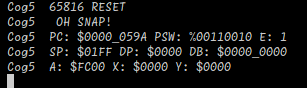
And it's already passing loads of tests as 65C02 (including illegal BCD) in E=1 mode. There doesn't seem to be a 65816 test program, so that'll be hope and prayers for now.
Had to add wraparound for direct page addressing in emulation mode for it to pass. I feel like that's just a waste of an instruction (I'm pretty sure every SNES program will switch to native mode immediately and never look back), but oh well.
Nice fast progress Ada!
Yea, it's going pretty good so far. Need to implement PSRAM functions and memory mapping next. But right now it's nice outside and I'm sitting with my thinkpad under the cherry blossoms.
For PSRAM, i'm going to use the same queue idea as the 68000 core. Though I think in this case it'd become easier if JMP/JSR always force reload it (even if the JMP would have been in range). Any JMP-type instruction is at least 3 bytes long, so there's a 3616 -> 288 cycle budget there.
Since I decided that all data access needs to be broken down into bytes, a simple cache may be needed for ROM data reads such that 16 bit reads (and block moves) aren't extremely slow. Though block moves are supposed to be super slow I guess.
In memory mapping, I think it may be easiest to have a kind of overlay system where the code for a particular cartridge type is slotted into a hole left in cog memory, because there's at least 5 or so types:
(HiROM will place NVRAM/DSP in the $6000-$7FFF expansion area, that I think needs to be handled, too)
So glad to see this happening...I know at one time you seemed pretty staunchly opposed to writing an SNES emulator (it sounds like it's more of a pain to write than your other emulators were), but thanks for writing it! I have a lot of fond memories as a kid of going to a more affluent friend's house and staying up late playing SNES games.
Cheers
Oh, I remember saying something like that maybe. Consistency isn't one of my strengths.
It is far more of a pain. As far as the video side of things goes, SNES really needs super cracked code on top of even higher clock speeds to work.
Maybe don't celebrate too early though, it's not working yet. Wait until I can get some corruption vaguely resembling Super Mario World on-screen")
Anyways, greetings from under the aforementioned cherry blossoms.

Nice day! Definitely nicer than the currently gloopy weather here... Looks like a really nice spot to hang out, too...
Need to work up some motivation to deal with the PSRAM stuff. The code I can copy in from MegaYume is a minor mess as a result of originally being written exclusively with the EC32MB in mind (longword addressing and all) at first and then extended to deal with other memory types later. This is somewhat unfortunate in the sense that the options that are slower to begin with are further slowed down by overhead. Since the 65816 is so byte-oriented (and can in theory crank out memory transactions much faster), I think something significant is gained if everything starts out with bytes.
Also, the code I have transparently splits transfers across pages. This is undesirable for data cache use (since the second transfer may end up not actually being used). So the idea would be to never cross pages for data reads and have two registers indicate the range of currently cached memory. That way the second read only happens when necessary (which one would hope is statistically unlikely enough to not cause problems). Since page boundaries also align with 65816 bank boundaries, this should also prevent oopsies where data is cached in an inappropriate manner (i.e. if reading a byte from $7DFFFF, this would not cause $7E0000 (a RAM location) to inadvertently end up getting mapped into the PSRAM cache because it would not go across the page boundary) EDIT: Thinking about it, that wouldn't happen, anyways, since cache check has to happen after address remapping (obnoxiously)
Probable cache sizes:
The 65816 itself can read 3 consecutive data bytes at most (and only from stack or DP, which are unlikely to be in ROM), but the DMA controller can do 5 when doing direct-mode HDMA with 4 byte transfer size. However, that particular case is unlikely and most HDMA is from RAM, anyways. If the 4 bit PSRAM had to use the same caching as the 16 bit, it would need 32/48 fetch cycles, which would make it slower than it already needs to be.
The code caching strategy should be the same as MegaYume/NeoYume, except byte-oriented. (the 68000 core does not use a data cache at all, btw. However, 32 bit access is performed as a single operation)
Do you need to ever write to PSRAM at run time from the application (after game is loaded), or is the PSRAM only for ROM emulation (therefore read-only) and RAM spaces for the 665816 gets mapped to HUB? I'm unfamiliar with the system aspects of the SNES memory and its HW surrounds.
If you do need to write CPU data to PSRAM yeah you'll need to deal with read-modify-write stuff for memory transfers that are not natively sized. The end of row only complicates things further there as well and hits performance in those cases when unaligned. If you are caching data as well as code memory then maybe you can do a write back only when some existing/dirty cache line is required for the next reads and at this time you'll know the entire line's contents so don't need to do the additional reads before you write. That could simplify things but at the expense of maintaining a cache. But given the high transfer rate there should be an improvement vs additional access cycles, despite sending more data, plus you are caching anyway and should get some locality benefits if the cache size is dimensioned nicely.
It's ROM emulation only, as usual. So no need to worry about RMW or inconsistent state.
Cache needs to be super tiny since what really matters is the worst case, which is randomly reading single bytes. Everything has to be locked to the video timing, otherwise raster effects will fail to appear correctly. And SNES is like the third coming of Atari Jesus in that regard (Amiga was the second).
Still no idea how exactly I'm going to handle H-DMA and positioned IRQs (you can set IRQ to fire at exact X/Y positions!) together. Technically HDMA should even be able to start mid-instruction. And at least one game actually would need this: Speedy Gonzales in Los Gatos Bandidos has a bug wherein hitting a certain switch in a rather late level (of course) starts waiting on a flag to be set in a memory location that doesn't exist. This only works because HDMA eventually interrupts the CPU just before it tries to read the value, so instead of getting the stale opcode byte, it gets a stale byte of whatever HDMA was reading, which eventually satisfies the loop condition. Though that's incredibly obscure, is it not? Probably not worth the headache (if you really want to play that particular game, someone made a patch to just fix the bug)
Point is, this stuff is rickety and needs its timing to work properly to not immediately open up a sinkhole directly to bug hell. I actually want to implement proper speed limiting here (the 68000 doesn't have it). Proper in a long-term sense, that is. I can really only do it on a per-scanline basis.... So did you know there's a SNES game that needs sub-scanline timing to work? Air Strike Patrol! Though that wouldn't work, anyways, since there's no way to tell the PPM cog that INIDISP changed mid-scanline. Or rather, is going to change, since it lives 2 scanlines in the past.
Basically: Everything's mega scuffed and compatibility will be bad (well, worse than it already is when we rule out SA-1, SuperFX and other heavyweight cartridge chips)
Unrelatedly, Hub RAM may be somewhat tight when all is said and done.
In terms of total RAM areas, there's:
Add to that the bloat from the Spin2 upcode... Which could be reduced dramatically if flexspin's nu bytecode backend was actually functioning. Oh well. Might have to go on a libc de-bloating spree. Oh well.