Requesting Peer Review of my RV-3028-C7 Board Design
in Propeller 2
As the title says, I'm ready to get some feedback on this board design. I have never done this professionally so I'm looking for feedback from individuals who have produced production boards. Thanks.
I doubt I'll produce this board. This is merely a design exercise.
Design Goals:
(1) Duplicate all the functionality of the RV-3028-C7 Development Board from Micro Crystal onto the smaller P2-ES Eval Accessory board format used by Parallax.
(2) Use a two layer PCB with all signal and power traces on the top and the ground plane on the bottom.
https://www.microcrystal.com/fileadmin/Media/Products/RTC/Demoboard/RV-3028-C7_Demo-Board.pdf
Functionality:
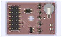
(1) Breakout - The RV-3028-C7 only requires 5 signal pins. This header provides access to the remaining 3 unused pins. It also provides access to 3V3, 5V and GND.
(2) VDD Jumper - This header allows the board to use either 3V3 or 5V as the VDD.
(3) VDD Sense - This header is mainly used to allow the connection of test equipment to monitor current draw of the RTC.
(4) LED Select - This header enables/disables the LED especially when testing the current draw of the RTC.
(5) EVI Select - This header allows the EVI pin on the RTC to be pulled up or down as needed.
(6) VBackup - This header allows the use of up to 3 different backup power sources or a pull-down resistor.
CAVEATS:
(1) All headers pins are 1 mm pitch!
(2) There might be a problem pulling the EVI pin up or down while connected to the P2 pin!
(3) Not sure it would be wise to use the 5V source as VDD while connected to the P2. Provided merely to satisfy design goal (1).
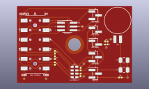
Both schematic and PCB have passed all DRC checks.


Comments
The traces which squeeze between the alignment holes of the large header seem like they might be better off running on the other side of the board. This is likely just personal preference and your design is fine.
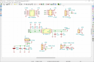
A comment about the schematic. It’s a poor way to do a schematic as it’s difficult to see where connections go. You board is simple so you should connect all lines so it’s easy to see what is connected to what.
Power and ground tracks should always be wider. Probably not an issue with your board.
I stick to 0603s as they can still be managed with manual assembly but I use 0805 for LEDs with a shorter footprint because 0603 LEDs are too fiddly. You have plenty of room on your board, use it. Those 100uF are way over the top, just use a 10uF. Whatever you do on the standby supply should contribute as little as possible to any leakage current. Remember the rtc is spec'd at 40nA, that's way low, keep it that way.
Make your pcb a touch longer on the connector side for that track that is running close to the edge.
I just use a 4-way 100k resnet to loosely couple the INT and EVI to the P2 but either way the EVI is a floating input and you should pull it down even if it is connected to an I/O which may be floating too.
btw, 10k pullups on I2C are fine for short distances and slower speeds. I use the P2's internal 1k5 source mode and run at 1MHz bus speed.
The RV-3028-C7's app manual (see image) recommends a 100nf decoupling cap on Vdd and Vbackup.
(1) I don't understand why you would put a decoupling cap on the Vbackup supply? Their own development board (see images) does not follow this recommendation. It doesn't use one which make sense to me.
(2) Why a 100nf on Vdd? @"Peter Jakacki" recommended 10uf and that's what they use on their development board and I've used in my design.
Are these just typos?
The other issue, I missed the first time through, was their recommendation to tie the ~INT pullup resister to Vbackup (if using the ~INT while on Vbackup). Not sure how to deal with this yet.
I've attached an update to my schematic (see pdf) per @Cluso99 's recommendation.