The NCD 40-Pin DIP P2 Board
 Dave Hein
Posts: 6,347
I've started playing around with KiCad to see if I can design a 40-Pin DIP P2 board. The board would be similar to the P2 EDGE, but with only 32 I/O pins and a DIP connector instead of an edge connector. The DIP connector uses 0.1" pin spacing with 1.1" or less between the rows. The goal is to have a board that can plug into a wireless breadboard with the hobbyist in mind.
I presented this concept before by hijacking other people's threads, so I thought it was time to start a thread specifically on this concept. I've never used KiCad before, so I'm learning as I go. I've only designed one PCB before using Eagle.
Thanks, to Cluso and Peter for helping me to get started on this project. I also want to thank Tubular for discussions that we've had about the P2 board he is developing.
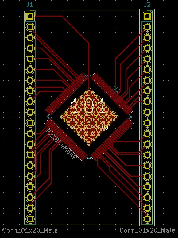
I've downloaded and installed KiCad and added Cluso's P2 KiCad library file. This is what I have so far.

The board size is 1.2" by 2.0". I've only connected GND, P0-P7, P16-P23, P32-P39 and P48-55. I still need to add 1.8V and 3.3V regulators, flash, bypass caps and a 4-pin Prop Plug header.
I presented this concept before by hijacking other people's threads, so I thought it was time to start a thread specifically on this concept. I've never used KiCad before, so I'm learning as I go. I've only designed one PCB before using Eagle.
Thanks, to Cluso and Peter for helping me to get started on this project. I also want to thank Tubular for discussions that we've had about the P2 board he is developing.
I've downloaded and installed KiCad and added Cluso's P2 KiCad library file. This is what I have so far.

The board size is 1.2" by 2.0". I've only connected GND, P0-P7, P16-P23, P32-P39 and P48-55. I still need to add 1.8V and 3.3V regulators, flash, bypass caps and a 4-pin Prop Plug header.


Comments
There is a KiCAD plugin called WireIT
https://forum.kicad.info/t/wireit-pcbnew-plugin-for-adding-cutting-swapping-wires-in-the-physical-layout/11212
that allows free-form trace connect and net-name, without a schematic, which can be useful for quick concept checks.
Some tips around OSC choices
* The P2 can drive ok from a clipped sine oscillator, which have much better precision than xtals. A simple AC coupling cap is all that is needed. Can become a low value R for CMOS osc.
* There are some thermistor crystals available, which usually have pin 2-4 as thermistor so GND=Pin2 and Pin 4 = P2 pin or uncommitted can support those as an option.
* Murata have sub-ppm oscillators in CMOS and clipped sine, in 5032 packages
* A mid-price solution can be something like ECS-TXO-2016-33-200-TR ~2ppm 3v3
When you get there, do think about using the optional transistor reset and the standard footprint for either USB-TTL CP2102 6-pin full-size USB or the micro USB version (yes, they change the footprint!) which are only ~$1.50 shipped on fleabay. Or talk to Peter about a cutdown version of his UB3 for onboard USB.
BTW I do see at present you're at 1.1" pitch! Not much space is there? I really admire you giving it a go!
KiCad tip - use "X" to start track placement after you've "Esc"aped the previous routing and had to abort it. Saves moving the mouse up to the right panel and select the track again.
I use inches to define the pcb outline and pin headers, and metric elsewhere. If you do this, then use 0.13mm as minimum track/space which is just over 5mils. I used to layout my pcbs in imperial 6mil (previously 8mil) only. I changed when I shifted to KiCad.
KiCAD has a nice shove router, which I think is why the add-on auto-router was deprecated.
On lower layer counts, placement and pin-swap and part nudge all interact to help routing yields, but all that is manual.
My first attempt was using the 1.1" pitch without rotating the P2. I was able to route it, but the routing looked messy, and I was concerned about placing the bypass caps. Once I figured out how to rotate the P2 45 degrees it made the routing much easier.
At this point I'm only using one side of the board. I haven't gotten to the point where I can use vias, and take advantage of both sides. I'm still learning.
There is usually room to allow > 1 oscillator footprints, which means user choice can come for free.
2016 and 2520 packages can usually be supported on one adjusted footprint, and simple solder bridge jumpers do not take much room.
Note that a plain vanilla crystal is going to limit timing precision to about ~16 bits, which seems poor on a part able to run ~200MHz with many 32 bit timers.
Only 5 of the 6pins need to be connected as the 3V3 is unusable. The advantage is that you can power from the USB (PC) or just use it to power the 5V/GND too.
Looks good, but SOT23 regulators are quite poor thermally.
A thermal pad part is going to get the heat to the bottom layer much better.
A part like NCP187/NCV8187 is low noise, with PowerGood and in 2x2 or 3x3 packages.
The biggest PAD package that can fit in the space will give the best thermal spreading.
You need a few resistors
- Reset (pin 100) needs a pullup, unlike P1
- The chip select of flash could probably use a pullup, too
And the test pin, pin 1 should be connected to gnd
Ground pad isn't very big to get the P2 heat away.
Not much bulk/bypass caps.
Looks like you're having fun tho
I only have 4 decoupling caps for the 1.8V supply, and it shouldn't be too hard to increase this to 8. I'll probably go with a switching power supply for 1.8V. The linear regulators are really more of a place holder at this point.
I haven't figured out a good way to connect the P2 ground pad to the rest of the ground copper pour on the bottom layer. Currently I have only one ground bridge at one of the corners. I can probably connect the P2 grounds on all four corners, and feed the 1.8V in from the top layer using vias.
I'm thinking of going to 0.9" spacing by eliminating the 2 center pins on each side. It looks like that should still be wide enough to accommodate all the parts, and I think it can still be routed in 2 layers. I'll stay with the 1.1" spacing for now, but maybe reduce it to 0.9" once I've fixed the other issues.
How important is that small width change ?
It seems better for a DIP-40 design to be as form compatible as possible with FLiP-P1 which does use all 40 pins, and then a very simple mechanical adaptor can manage a 0.6" conversion, if someone needs that.
Matching those inner pins is more important. So long as the pins match, simple formed headers and DIP sockets could be used to make a 0.6" adaptor.
There may be room to fit a USB connector for 5V power ? (and maybe DP,DN for P2-USB use ?)
There may not be room to fit a UB3, but maybe with time, a P2-Device can go into flash to allow some self-boot ?
There are low cost MSOP10 MCU that could fit for smarter boot ?
Addit: Maybe this MSOP10 CH340E can fit, to give vanilla USB ?
This is a 1.8A rated micro-USB with 4 full length stakes
The 1.1" version will fit in a solderless breadboard, but it does require running wires under the board. 0.9" is better because it does allow for one outside row on each side. That will make it easier to wire up I/O pins on the breadboard.
I'm still thinking of using a switching regulator for 1.8V. It just seems that dropping from 5V to 1.8V using linear regulators is very inefficient, and they're going to generate a lot of heat.
* The TAB is not grounded, so they cannot connect directly to a plane
* They lack a Power Good Signal.
* Output noise is high at ~ 60uV/V
The NCP187/NCV8187 cost a few cents more, but have a GND PAD, and do include a PGood and are low noise.
Yes, the simplicity of chained linear regulators, comes at a high thermal cost.
Possible conservative (3A) Switching Regulators are AP3441 and TLV62585PDRL, and I selected the TLV62585PDRL as it has lower RDS on the FETs and allows a slightly smaller inductor.
Both those parts have PGood.
As room allows, you can also 'oversize' the switching inductor, as the larger ones have lower losses per Amp.
I'm currently pursuing the idea of doing a DIP adapter board for the P2 Edge. This is more in line with my soldering capabilities. I've attached pictures of the 0.9" NCD card and the P2 EDGE adapter card.