P2QT - P2+regs+Flash+uSD in a 68-pin 0.91" sq Quad "Fat" Pack
 Peter Jakacki
Posts: 10,193
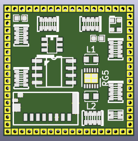
Cluso99 posted a bare bones P2 module but I wanted a really small module too with just the minimum number of pins for the 64 I/O, plus Vin, ground, Vout, and reset, so 68 pins and 0.91"sq with regs and Flash etc. However I decided to put the P2 on the reverse just by itself and still have uSD, Flash, and switching regs on the top side. This is my P2QT. Am I crazy? Yes!
I want this board to integrate into a legacy design and also check a new dual 2A switching regulator plus I'm using cap arrays as well to squeeze it up a bit more. It's a wip but one I will get done. So there is no USB or RTC or clkgen options or LEDs etc so this will be an easy board to manufacture. The uSD header faces in just like it does on the P2D2 and the card slides in over the top of the Flash.
The corner pins are reset,power,ground,3.6vout, with 16 I/O on each side. The pcb is 0.91" sq (23mm x 23mm) and might end up 4 layer. If this goes onto a pcb I can also cut out a place for the P2 chip to poke through just to get it flush.
Don't expect to plug this into a breadboard, but you can prototype with it using my microMAT boards with the 50mil pitch dual hole size pads. The P2D2 on the other hand is ready to run when you plug in the USB.
Here's a rough layout and I will edit this later to show the components. If the holes are castellated then it could be surface mounted provided there is a cutout for the P2.


Comments
It seems like a great minimalistic board; it really is a cutie (QT?). We're going to need that, something that can hopefully sell for $30 or so in quantity one, and something so compact, yet straightforward to connect up with. The features of Cluso's board overlap, but it's good to have options.
I didn't know about cap arrays. Those should be easier to pick-and-place (if doing so manually, I mean). And if wanting to surface- or flush-mount the P2QT, there's a good chance that the folks designing carrier boards for and around it will be able to include a board cutout for the P2 package.
Anyway, 16 I/O's on a side, 17 total pins per side, makes for a nice "fat pack" (but not too fat). A minimalistic board like this is kind of what I was expecting from Parallax. But their Edge board/card is nice, too. And there certainly is a place for it. But it does require a rather large card socket. And at $49 for singles (at least at present), it opens the door for other designs, which is fine as far as Parallax is concerned since it's their chip either way and "the more, the merrier" in terms of boards in the P2 ecosystem.
This board is closer to being a chip than a board, hence the "quad fat pack" in the title.
I suspect the castellation is a bit ambitious for the corner pins, if these handle the power. If you shave off along all four sides what you're left with in each corner is just 1/4 of a plated hole
Getting heat out will also be interesting, but hey lets try it and see
I've seen many edge designs use dual plated holes for that reason, and top and bottom routing to the edge pins.
My concern with my original double sided design that was components on both sides was too risky. I've done plenty of P1 double sided designs where the caps were better placed underneath. However, the P2 has that big ground pad underneath which probably means you need to solder it first. Then you turn the board over and solder the jelly beans and hope the P2 doesn't move - unlikely but I decided against it. I'll be interested to see how it goes.
@Cluso99 - I am relying on the P2 and its big ground pad to hold the P2 in place when it gets mounted and reflowed first, and after cooling I will stencil the top side, place components, and then the panel will rest on an insulating and support layer (during the second stenciling too probably). This goes back into the reflow oven and all should be good. If need be I could make up a dummy pcb with cutouts just to support the P2QT panel when it's flipped and reflowed.
@Tubular - I will either have to order these with through holes or get some made as a castellated version. It's true that the corner pads need special attention in that case but I will initially just make them as TH pads.
The P2D2 of course is a complete system especially because of the USB serial among other things.
You can get screened 0.025" pitch ribbons ok
Spectrastrip make a twist and flat ribbon, but I think i've only seen 0.05" pitch
https://au.element14.com/amphenol-spectra-strip/132-2801-016/ribbon-cable-16way-per-m/dp/1207478?
Unfortunately, it isn't at next corner store...
https://iec.net/product/30-gauge-68-conductor-025-inch-pitch-twisted-pair-ribbon-cable-for-scsi-lvd-320/
The proof of the pcb will be when I use it, and I will take it from there if need be.
Yes, I'd agree that a single corner gnd path on a 100+MHz digital part is 'optimistic'.
A 2.54mm nudge of PCB size would allow a centre gnd pin on each side, & would lower crosstalk effects, and that could free a corner pin for maybe EXTCLK in option ?