P2-ES Ethernet Dev Board Add-on
Hello Parallax,
Is there any plan to make a ethernet dev board add-on for P2?
I think that if parallax selects and provides a common board, then it will speed up development.
Is there any plan to make a ethernet dev board add-on for P2?
I think that if parallax selects and provides a common board, then it will speed up development.
[2021/03/21] Update:
- I bought Waveshare DP83848 and LAN8720 daughter boards, as no board from parallax is expected to come soon.
- I suggest to use DP83848 as it has option to use RMII 1.0 (see comment #21 for CRS_DV and RX_DV signals).
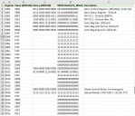
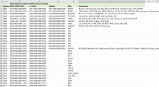
- Implemented MDIO test code to read registers from PHY Address 00001 (default DP83848, LAN8720 address).
The test code matches the TI Launchpad MSP430 USB-2-MDIO SW tool (https://www.ti.com/tool/USB-2-MDIO)
[2021/04/10] Update: Added write function. We can do software reset to DP83848 by just writing bit 15 on register 0. )
[2021/04/21] Update v0.4: Added new options to select PHY (option 3) and REGISTER (option 4). It is now possible to write and read any register on any phy and dump the results. (Issues with read are not yet solved, will need to do more debugs)


Comments
The Wiznet 5000/5200/5500, ENC28J60/ENC624J600 or similar IC helper solutions are not optimal for many reasons
Those Wiznet 5000/5200/5500, ENC28J60, etc... ICs are limited to they internal fixed architecture. They were born in the first place to help Low performance MCU to have Ethernet connectivity. Have limits on performance, number of TCP/IP sockets, etc ... It is not flexible.
A MAC/PHY directly 'read/write' ethernet frames into the wire. It is completely flexible (able to develop any protocol). You are 'read/write' at top line wire speed (97 Mbps).
With a MAC/PHY you can DEMO/SHOW that the P2 is able to fit the space between a high performance MCU and FPGA. And beat them both due to easy of programming, flexibility to develop any protocol, and top wire speed performance.
I see the W5500 data claims this
"The W5500 SPI supports 80 MHz speed and the new efficient SPI protocol, so users can implement high speed network communication. "
The W6100 data claims 70MHz SPI speeds.
https://en.wikipedia.org/wiki/Media-independent_interface
Of course we can't actually clock the P2 off the 8 GPIO pins each module feeds directly to/from the P2-EVAL, that would need to be jumpered somehow to control the P2 clock which gets messy.
I wonder what other common MAC interfaced buses use? QSPI could be handy for Fast Ethernet but wider parallel bus solutions will restrict their use once they exceed 16 pin capabilities of the double wide P2-EVAL modules.
Also before these such Ethernet modules are usable on the P2 you'll need a low level MAC and/or PHY driver and very probably an IP stack too (depending on what you want to do with Ethernet).
Oh yes
I am waiting for the P2D2 with development board or could use a spare IoT5500 to port the scriptable dynamic webserver I had for Spinneret under Tachyon 3.0 to Taqoz
Or maybe first port it to Tachyon 5.x when I have a bit time in August
The purpose of this thread is to know if Parallax is willing to choose a PHY, design a board, and sell that Ethernet Add-on Module as extra for P2-EVAL board ... to have some kind of reference design, and to avoid duplicating software efforts ... that will help Parallax to say 'look I can do all of this so simple with just one P2, a cheap common PHY, and some smartpins'.
So I suggest to use directly a PHY IC. With Hyperram/Hyperflash it wasn't a big problem to choose specific which specific IC (there were just two manufacturers, and a few parts). But with ethernet PHY is more difficult as there are many options.
About PHY interface. Probably there are just only two options out there:
1) RMII
System clock can be P2 or PHY
Clock frequency : (50 MHz +/-50ppm) for both 10Mbps and 100Mbps
Total number of pins required: 10 pins (8 for PHY + 2 for MDIO/MDC)
2) RGMII
There are two clocks : TX and RX clocks (and are dependent on speed)
Clock frequency : 2.5 MHz, 25 MHz, 125 MHz (for 10 , 100 and 1000 Mbps modes)
Total number of pins required : 14 pins (12 for PHY + 2 for MDIO/MDC)
The board will need to be plugged into two 2x6 headers due to number of pins (just like hyperram board).
The need to choose the PHY IC is because every PHY on the market needs to be configured via two pins (like I2C, but called MDIO/MDC) at startup and that code might be PHY dependent.
But other that those two MDIO/MDC pins, the other pins (8 for RMII, or 12 for RGMII) follow a standard. So the software coded for this part is common for every PHY on the market (usually called MAC). And that is the reason that I think it would be better if parallax choose one IC component and make a board and everyone else develop a software on that board.
Is it parallax here? @Ken @cgracey @VonSzarvas ? or do I need to send the question to support?
Will need to digest all the ideas in this thread and understand what would be the most useful configuration for most users.
For example- if the 8 pins are the main requirement, and those extra 2 are only for 1-time configuration, then maybe this could be a single-header accessory and have a 2-pin jumper cable to another edge header for the occasional configuration need. OR maybe share 2 of the 8 pins and have a dip-switch or jumper to swap into configure mode, instead of a jumper cable... (that assumes all 8 I/O's are not needed during the configuration step).
You mention RMII and RGMII ... which would you choose ?
Those two MDIO/MDC are always usually needed even if the application is simple because that is the only way you can check link status (up/down), set speed/duplex mode (10mbps-duplex, 100mbps-HalfDuplex, 1000mbps), check counters, and many other things (like reset) ... BY SOFTWARE.
Usually the PHY can many extra pins to configure the speed mode, and duplex mode by (pullup or gnd connection). This is usually called hardware configuration. I don't think it is flexible for a development board so I suggest to have two dedicated MDIO/MDC pins. However there will be no problem to reserve some jumpers to allow hardware configuration IF there is board space.
So a RMII 8 pins board with hardwired modes (user selectable) might be possible but if will require the user to change a jumper every time it wants to change from 10 to 100, or from half-duplex to full-duplex. And will mean no way to have statistics (number of packets, errors, etc ...).
Between RMII or RGMII, I honestly don't know what will choose due to clocking. By the way, I miss that the P2 board doesn't have a socket for common 3.3v DIP oscillators (half-size DIP8). Also, RGMII use double data rate (DDR). I am not familiar enough with P2 to know if smart pins can handle it, and if they can handle external clocking for RX that has a different phase from the P2 clock TX clock (as RGMII has two clocks). RMII specification says that the clock can be dictated by either the P2 (the call it MAC) or the PHY (which will limit somewhat usefullnes to P2 board). Datasheet needs to be checked carefully. Other PHYs maybe can do clock recovery from its received TX (from P2) and synchronize the RX clock to that TX clock and use buffers fir RX data (from wire cable). I remember that TI 'phyter' said something related about this.
So it requires some study and discussion to check what both PHY and P2 can do.
In case of doubt, a call to some PHY manufacturer FAE saying that you want to ship a development board - worldwide - as reference design ... with their chip on it ... might help a lot in the design phase of the board.
For Fast Ethernet support only I would think RMII is much easier to sort out the clocking. The Wiki page I linked above mentions this about RMII REF_CLK:
"Reference clock may be an input on both devices from an external clock source, or may be driven from the MAC to the PHY"
This means in theory the P2 could supply this clock from an IO pin.
Supporting Gigabit Ethernet using common PHYs on a P2 with a 16 pin limit you'll need to use RGMII but it will be a challenge with the receive clocking from PHY->P2, clock variation with link speed, and the RX framing. From a streamer perspective it's probably looking somewhat like the HyperRAM with DDR, but the receive control signal timing may be tricky. It looks like you need to continually stream data in and later mark frame start points in memory because the data valid signal comes in with the data itself, you can't use it to trigger the streamer it's too late by then. RGMII also uses lower voltages and so would require level translation though that is probably a very simple issue to sort out.
Check just DP83TC811R-Q1 as example, but almost all other PHYs are the same.
So it is possible to have both interfaces as option (but not working at the same time) within a single board.
*A quick check at lcsc finds these product lines
SMD Oscillators(XO) (2235) DIP Oscillators(XO) (11)
Maybe
https://www.microchip.com/wwwproducts/en/LAN9252
or
https://www.ti.com/interface/ethernet/phys/products.html?pqs=paqs&familyid=1752#p2192=IEEE 1588 PTP;IEEE 1588 SOF
I found and bought some ready made boards. LAN8720 and DP83848. Haven't tested them yet.
My programming skills are close to zero. I would appreciate if someone could help me to create some rough test or skeleton code for them (in whatever language that make the ethernet frames flow).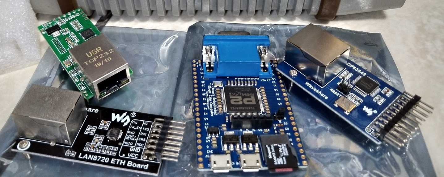
That DP83848 based board looks interesting and its schematic appears to have the OSCIN signal wired too so you might be able to mod it by removing R1 and sourcing the clock from the P2 for RMII operation. It also has the RX_DV signal available too at R9 which you could wire to the NC pin and this could simplify the receive process for the P2. If you can live with the default PHY settings you could make an adapter to use a single wide expansion board for the P2-EVAL, but having access to the two MDC/MDIO signals will help to debug a lot, so a double wide adapter board is better. I would recommend aligning RX0, RX1 on an eight bit pin boundary for the streamer.
When I worked in data networking we had to bring up Ethernet PHYs all the time, they were never that trivial to do so as each one seemed to have it's own set of quirks and auto-negotiation was often troublesome. That was 20 years ago so hopefully things have become simpler since then and it might be easier now....
I second that. Being able to implement an EtherCAT master or slave would be a great benefit.
I also sell CNC controllers which use their own protocol instead of TCP/IP. I think the Wiznet 5500 has some "raw" packet mode to bypass TCP/IP. But why use a complicated chip just to bypass almost all of its capabilities eventually?
I am having lots of fun and fustration (but second one is just my fault, not knowing how to code what I have in mind).
I have an awful but working test code for MDIO register reads for both LAN8720 and DP83848 daughter boards.
I will update the first post just to help us (everyone) into a much faster development (even if the code is ugly) instead of waiting a few weeks trying to get into 'divine perfection' ... that might could be years (remember P2D2!).
My suggestion for someone looking into which board to buy is to get the DP83848 board instead of LAN8720 (or both if budget allows). Nothing wrong with LAN8720 IC, but after carefully reading both datasheets the DP83848 explains that it supports RMII 1.0 protocol:
DP83848 default mode is RMII 1.2 spec (instead of RMII 1.0). Why RMII 1.0 is good? Well, for two reasons:
1) By default, the CRS_DV pin (in RMII 1.2 mode) could toggle at the end of frame. Making RX receive P2ASM/SPIN coding difficult.
2) Unfortunately, Waveshare designer didn't connected the RX_DV pin into the 0.1" pin header. That could have help to solve the problem. With RMII 1.0 mode (instead of default RMII 1.2), the CRS_DV pin will behave exactly the same as the RX_DV pin.
Additional info: National / Texas Instruments AN-1405 SNLA076
Here goes some ugly code that can read and display the MDIO registers (clause 22 only).
Special THANKS goes to the free TI MSP430 MDIO SW Tool (https://www.ti.com/tool/USB-2-MDIO) for being able to compare the actual output from both daughter cards with my P2 code, during testing.
Unlike the MSP430 tool (that depends on Windows only SW), this program try to implement a driver-less and OS-agnostic serial terminal interactive menu to select field values and commands. Unfortunately current code only can do reads and it is 'hardwired' to PHY address 00001 (both LAN8720 and DP83848 are hardwired to PHY 00001 Address).
I wanted to implement both READ/WRITE, and be able to select PHY ADDRESS and other values, but due to lack of time I release this early AS-IS to speed up development.
On the Waveshare DP83848 board I think it would be rather easy to solder the RX_DV signal to the 0.1" pin header. This may allow better synchronizing to the incoming RXD preamble (if they are aligned in time) and using this pin to trigger the streamer to start receving data. Without that signal, if the edge of CRS_DV varies relative to the preamble start then further decoding during transfer is required to identify the actual SFD position in the captured data stream. However because the CRS or CRS_DV signal (Rev 1.2) is able to be dropped off when you lose carrier in the middle of the packet, unless this signal is also monitored the only thing that let you know you are receiving garbage is the CRC. The streamer will need to be stopped whenever the RX_DV drops too, and also if once some maximum allowed jumbo size is received and needs to be truncated.
In either case, I imagine Ethernet frames will need a bit of extra space around them in HUB RAM to hold some leading preamble/SFD and any trailing received data before the streamer shuts down. The RX COG will also need to compute and store the packet length based on when the RX_DV drops. A smartpin mode might be able to time the clocks while the RX_DV signal is high and use this information to compute the length.
Yes it could be easy to solder some green kynar wire to the header. But probably we might not need it.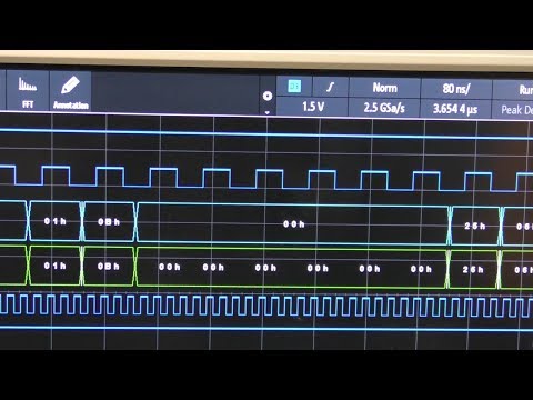
Please check this video from Mikeselectricstuff (Sep 1, 2018) ->
No need to watch all 30 minutes. Interesting talk starting from 15:52 up to around 24:00
Specifically, Data_Valid synchronization start issue -> 16:40 - 18:22
Synchronize when all (CRS_DV & D0 & D1) are High
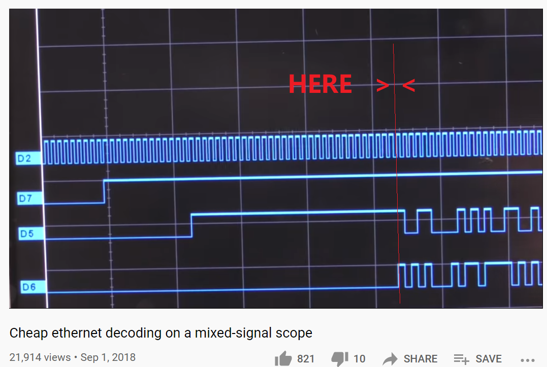
"That point we know it is a known position within the frame"
Neat video, clever use of data pattern to sync to SFD. This combined signal pattern is late though and would likely be too late to start the streamer. I guess you could do something like the following though...
1) wait for the first low to high transition of CRS_DV, timestamp it and start the streamer capturing bit pairs to HUB RAM
2) wait for the logic pattern high, high, high on RXD0, RXD1 and CRS_DV, or timeout
2a) if timed out, then abort streamer reception and wait for idle and restart
2b) if not timed out, capture exact P2 clock time and compute number of clocks since the timestamp so you can figure out real start of packet in HUB RAM as an offset from start buffer
3) wait for end of the packet by waiting for some time after CRS_DV drops low (tricky if muxed with CRS and toggles in RMII v1.2 mode)
4) stop streamer, write real packet start offset and length into circular rx buffer, and restart capture process for next packet.
But what about the packet's CRC check? I think you'd want to have something do that too. A COG could hopefully do it reasonably quickly with SETQ to read blocks in rapidly and process them with CRCNIB or a table driven approach perhaps. It would only take 384 clocks to read in a 1536 byte packet into COG/LUT RAM where it could be worked on, but the CRC test might slow down the reception rate significantly. Small 64 byte packets+IPG+Preamble can arrive every 6.72us in theory worst case @100Mbps. Be neat if there was a way the CRC check could be done in parallel with receiving the data somehow....? Maybe the TX COG could assist there if it's idle during receive...?
By the way for CRC, it might be possible to keep up at line rate if the CRCNIB instruction can be employed effectively. I've not checked if it could be used for Ethernet CRC (hopefully it can).
E.g. at 200MHz you have 16 clocks per byte for Fast Ethernet. You get to read in 32 bits in 1 clock with SETQ burst, then do two CRCNIBs for each byte. Even with extra loop overheads and internal register lookup etc, it might hopefully just fit in the budget, but I suspect it would get tight.
There is a variant of the CRC algorithm that uses a lookup table that should be fast enough
There is also a version of the CRC instruction that can calculate for each bit. Sometimes this can fit better as the bits are being assembled.
Although the ENC28J60 is limited because it is 10baseT, it is in fact general purpose and can form any protocol. I ported Harrison Pham's P1 drivers to FastSpin last year and uploaded them to the forum. It has the advantage of being entirely SPI and therefore needing only 4 I/O pins. For anything short of serving video it's hard to imagine why you'd need anything more performant.
Edit: I have had IIC on the brain lately. Of course it's a SPI device.
Here goes a real life (wire captured) ethernet frame:
Last four bytes (5B 00 6C 87) are the FCS.
The CRC is supposed to be this one:
  G(x) = x32 + x26 + x23 + x22 + x16 + x12 + x11
             + x10 + x8 + x7 + x5 + x4 + x2 + x + 1

  https://github.com/Michaelangel007/crc32
  https://stackoverflow.com/questions/2587766/how-is-a-crc32-checksum-calculated
I have seen that P2 has a CRCBIT and CRCNIB instruction, but I fear it is not the same as CRC32. How can we calculate the CRC?
It's mainly a matter of computing and setting the correct polynomial values in S for the CRC you are using then calling CRCNIB D,S with SETQ or use CRCBIT one bit at a time. You need to be aware of the bit endianness order too to present data and shift in the right direction that the P2 HW uses.