

I need help with ADS1015 12Bit ADC
 T Chap
Posts: 4,260
T Chap
Posts: 4,260
I am stumped on something and could use a fresh set of eyes. The ADS1015 is an I2C 12Bit ADC with 4 inputs. I set up the config registers how I want with FSR Full Scale Range 4.096 which means 2mv ( .002V) per LSB. The math is working out correctly at lower inputs. I can take the raw 16 bits data and bitshift right and multiply by .002 and the values are correct. But someone everything above 4.1V is getting chopped off and the MSB+LSB caps at %0111_111_1111. It never gets to 12 bits. I assumed a 12Bit ADC means you get a maximum of 12 bits of resolution!
The ADS1015 has 5V on VDD, with Ferrite bead in series right at the VDD and VSS pins.
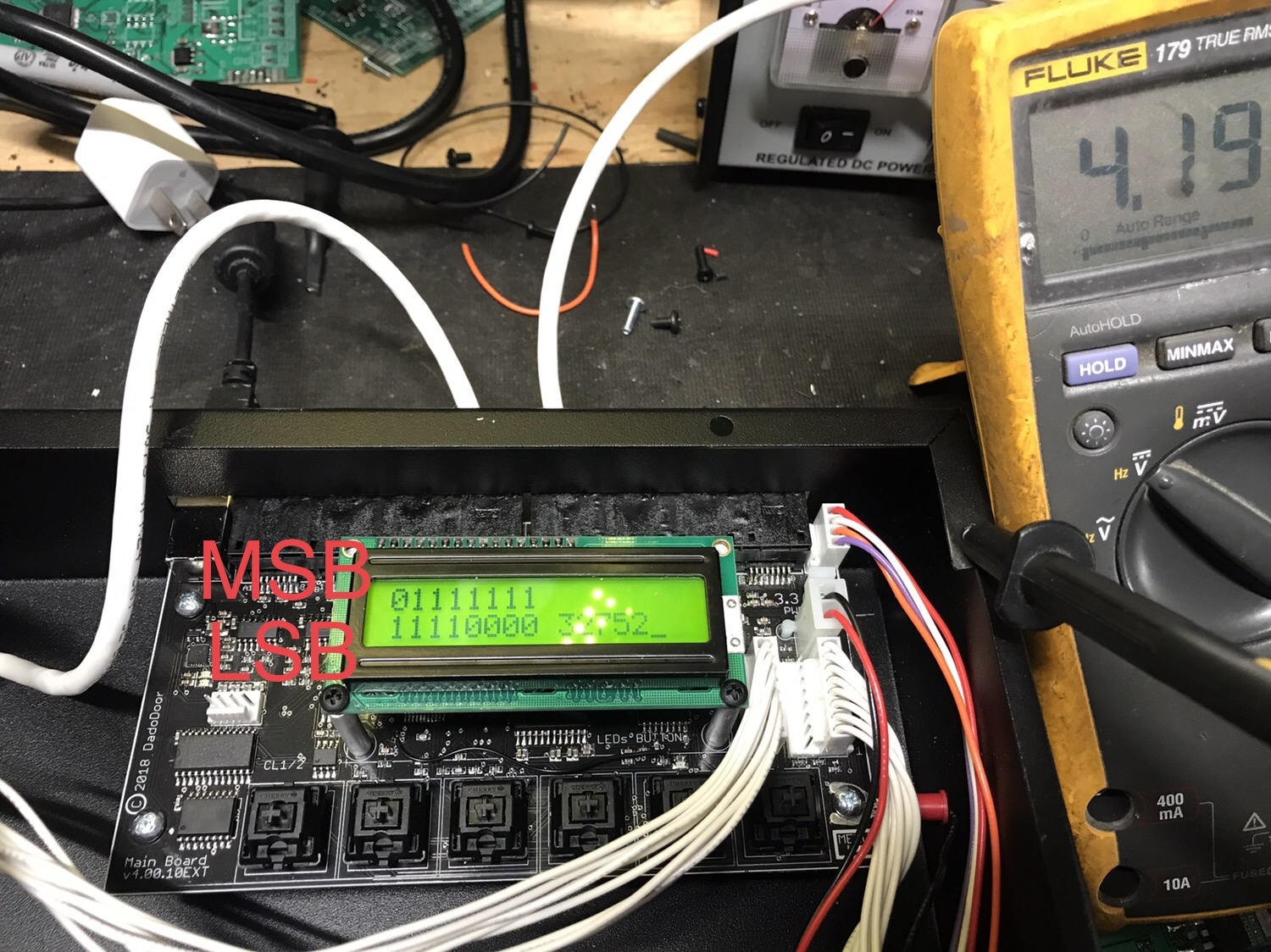
The maximum value at an input is VDD+.03, and I'm not getting close to that.
In the photo, you see the meter at just over 4V. The top row is MSB raw bits. The bottom row is LSB raw bits, this needs to be shifted right 4 bits to get rid of unused lowest 4 bits that are all 0's.
If I switch to Full Scale Range 6.144V then the ADC does not get close to maxing out with over 4V inputs. The main thing is why does the ADC stop at 11bits instead of seeing info in the 12th bit too. The decimal 2047 is the maximum I can see.
http://www.ti.com/lit/ds/symlink/ads1015.pdf
The ADS1015 has 5V on VDD, with Ferrite bead in series right at the VDD and VSS pins.
The maximum value at an input is VDD+.03, and I'm not getting close to that.
In the photo, you see the meter at just over 4V. The top row is MSB raw bits. The bottom row is LSB raw bits, this needs to be shifted right 4 bits to get rid of unused lowest 4 bits that are all 0's.
If I switch to Full Scale Range 6.144V then the ADC does not get close to maxing out with over 4V inputs. The main thing is why does the ADC stop at 11bits instead of seeing info in the 12th bit too. The decimal 2047 is the maximum I can see.
PUB ADCCONFIGInput1
     ' USE 4.096 PGA %001 for .002mV per LSB
     ADCconfigHigh := %1_100_000_0   '  OS[15]    MUX[14..12]      PGA[11..9] = %001= 4.096     Mode[8]  one shot
     ADCconfigLow  := %001_0_0_0_11    '  Data Rate[7..5]      CompMode[4]   CompPolarity[3]   Latch[2]    Comp Que [1..0] 11 : Disable comparator


 ' SEE BELOW FOR CONFIGURING HIGH AND LOW BYTES
     ' MUX SHOULD BE   100 : AINP= AIN0 and AINN = GND  for Motor1 Current Sense
     ' at INA138 inputs
     ' PGA  gain  001= 4.096 Highest   000= 6.144   010= 2.0148 Low
     ' A D C  C O N F I G    B Y T E S

     ' OS[15]   1  Start a single conversion
     ' MUX Inputs  MUX[14..12]
     ' 100   Single input 0-GND   <<<<<<<<#################
     ' 101   Single input 1-GND   <<<<<<<<#################
     ' 110   Single input 2-GND
     ' 111   Single input 3-GND

     ' PGA   gain  PGA[11..9]
     ' 000  Highest gain 6.144   3mV per LSB    TOO HIGH   1200 binary
     ' 001  Highest gain 4.096   2mV per LSB  BEST   .2V = 1600 binary <<<<<< YES>>>>>>>
     ' 010 2.048    too low        1 mV per LSB
     ' 011 1.024                      0.5 mV
     ' 100  .512                       0.25 mV
     ' 101  .256                       0.125 mV
     ' Mode[8]   0 = continuous
     ' Data Rate  100 = default = 1600 /SPS  001= 250 SPS  /    010=490  /  011=920SPS  /  000=128SPS /

     'MAX Voltage on inputs 0-3 ADC = VDD + .3   or 5.3V

PUB ADCRead
' A D C   R E A D   ADC  V A L U E
     i2c1.i2cstart(i2cSCL2)                                     ' START
     I2C1.I2CWrite(i2cSCL2, %10010000 + 1)         ' send device + READ mode   0 = WRITE  1 = READ
     ADC1 :=  i2c1.i2cRead(i2cSCL2, 0)                 ' read conversion MSB
     ADC2 :=  i2c1.i2cRead(i2cSCL2, 1)                 ' read conversion LSB
     i2c1.i2cstop(i2cSCL2)                                     '  STOP

' A D C  Combine result High Byte + Low Byte    12 Bit Result  XXXX_XXXX HIgh        XXXX_0000 LOW
     ADCsum :=    (   (ADC1 << 8)   + ADC2 )  ' >>  4

' A D C   Show Result
     CLS
     'go(0,0)
     ser.bin(3, ADC1, 8)
     go(1,0)
     ser.bin(3, ADC2, 8)
     'ser.bin(3, ADCsum, 12)
     go(1,9)
     ser.decf(3, ADCsum , 5)
     w(5_000_000)


{


Depending on the Full Scale you select, the measured voltage in binary will get multiplied by the LSB value to get the actual voltage it measured
6.144 = LSB  = 3mV     Default
4.096 = LSB =  2mV     Maybe use this.  Input cannot exceed 5V VCC
2.048 = LSB = 1mV
1.024 = LSB = .5mV

}


PUB ADCUpdateReg
     '1  Create 2 bytes for config based input 0 - 1, Full Scale Range for inputs 0 -1
     '2  Select the Config register to write to ( 01) then write the ADC Config bytes
     '3  Then select the conversion register since we will NEXT be reading ADC values
  ' A D C  WRITE  CONFIG  (SELECT  Input to Read 0-3)   MUST set the CONFIG based on which input to read
     i2c1.i2cstart(i2cSCL2)                                     '  START
     I2C1.I2CWrite(i2cSCL2, %10010000 + 0)          '  send device + write mode   0 = WRITE  1 = READ
     I2C1.I2CWrite(i2cSCL2, %01)                           '  Select register      00 : Conversion register        01 : Config register
     I2C1.I2CWrite(i2cSCL2, ADCconfigHigh )          '  Send Config byte HIGH
     I2C1.I2CWrite(i2cSCL2, ADCconfigLow  )          '  Send Config byte LOW
     i2c1.i2cstop(i2cSCL2)                                      '  STOP


' A D C WRITE CONVERSION REGISTER  (Tell Device which register we are working with = READ ADC CONVERSIONS)
     i2c1.i2cstart(i2cSCL2)                                    '  START
     I2C1.I2CWrite(i2cSCL2, %10010000 + 0)         '  send device + write mode   0 = WRITE  1 = READ
     I2C1.I2CWrite(i2cSCL2, %00)                         '  Select register      00 : Conversion register        01 : Config register
     i2c1.i2cstop(i2cSCL2)                                    '  STOP
http://www.ti.com/lit/ds/symlink/ads1015.pdf
1500 x 1124 - 479K
Comments
I use the ADS1115, which is the 16 bit version. It's full scale range is 15 bits in single ended mode. It might be a good drop-in upgrade for your setup if you need the extra bit(s) of resolution.
Perhaps this thread may help you, or maybe not.
https://forums.parallax.com/discussion/160328/configuring-a-programmable-gain-amplifier-on-an-adc