

[Beating a dead horse] Hybrid I2C/SPI Ram Expansion using SIMM.
 alatnet
Posts: 80
alatnet
Posts: 80
So, I had a thought of using external ram with the Propeller and saw a few threads talking about it.
Mostly it was either using only SPI or almost all the pins on the Propeller.
Well... Why not use a hybrid I2C/SPI setup?
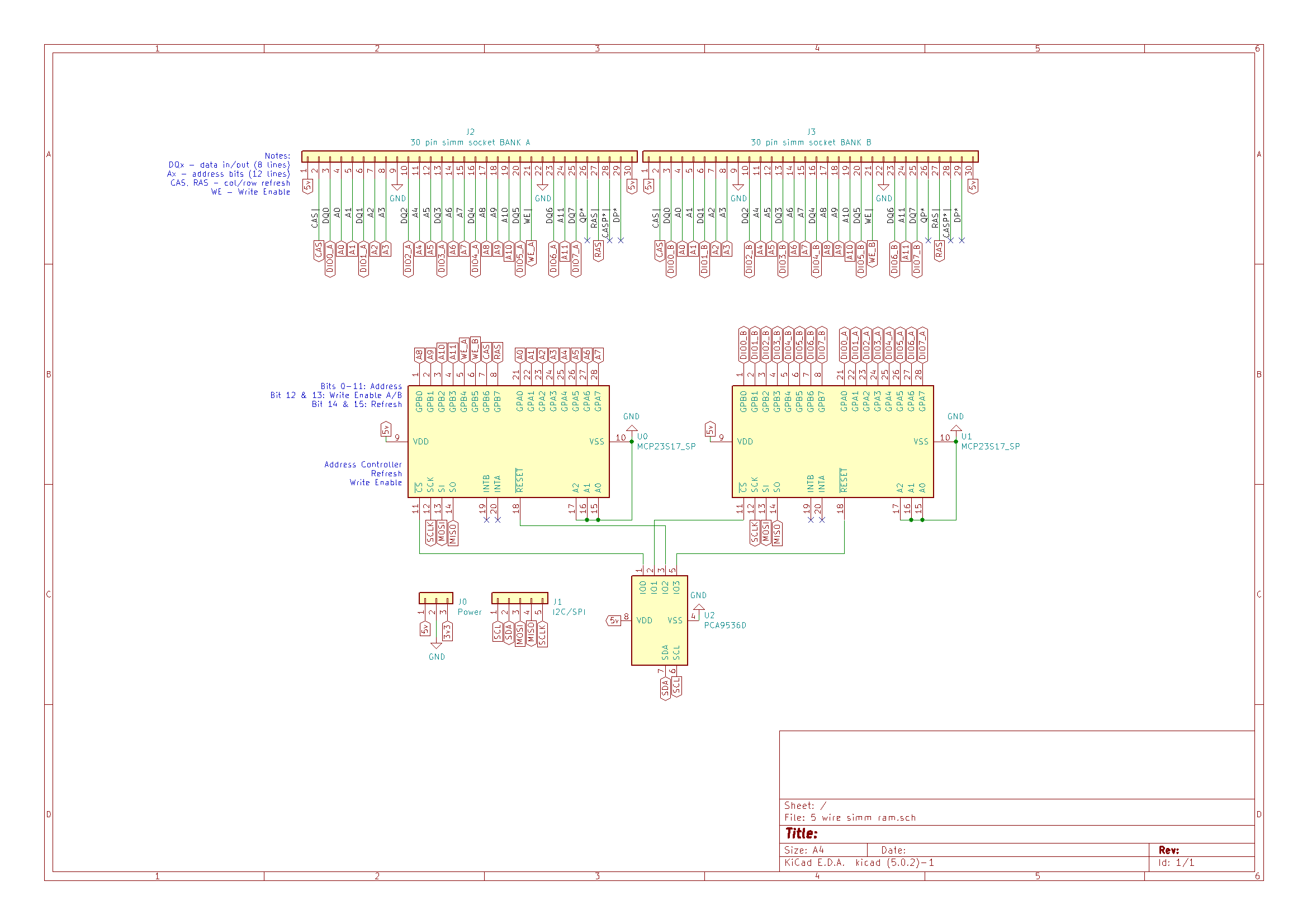
I've attached a drawing that I made to see if this is possible.
By using I2C primarily as a chip select between the two SPI chips, an address chip and a data i/o chip, it should be possible to have a decent amount of ram expansion while also having the speed of SPI for the data throughput.
I figured that using a SIMM module would be a decent bet for ram expansion as they can be more or less cheap and easy to use.
The best part of this, it only uses 5 wires off of the propeller chip. Though it could be trimmed down to 4 if you combine the clock pins of the I2C and SPI lines, though i dont know if that would cause problems.
Another bonus is that, with the right chip, you could, theoretically, have 128 ram expansion cards and with this design, 256 ram chips. In theory.
EDIT:
Just thought of this with my drawing.
Since the propeller chip is a 32-bit microcontroller and the data lines for each simm bank is 8 bits, the system can theoretically be used to split a 16-bit data between both banks.
And with a bit of modification to the drawing, can also split a 32-bit data between 4 banks of ram.
Mostly it was either using only SPI or almost all the pins on the Propeller.
Well... Why not use a hybrid I2C/SPI setup?
I've attached a drawing that I made to see if this is possible.
By using I2C primarily as a chip select between the two SPI chips, an address chip and a data i/o chip, it should be possible to have a decent amount of ram expansion while also having the speed of SPI for the data throughput.
I figured that using a SIMM module would be a decent bet for ram expansion as they can be more or less cheap and easy to use.
The best part of this, it only uses 5 wires off of the propeller chip. Though it could be trimmed down to 4 if you combine the clock pins of the I2C and SPI lines, though i dont know if that would cause problems.
Another bonus is that, with the right chip, you could, theoretically, have 128 ram expansion cards and with this design, 256 ram chips. In theory.
EDIT:
Just thought of this with my drawing.
Since the propeller chip is a 32-bit microcontroller and the data lines for each simm bank is 8 bits, the system can theoretically be used to split a 16-bit data between both banks.
And with a bit of modification to the drawing, can also split a 32-bit data between 4 banks of ram.
2338 x 1653 - 92K
Comments
You can "stack" 8 MC23S17 on one CS+SPI without other means. Just give them different addresses with the A0/A1/A2 pins. That'd give up to 128 IO lines per CS line without additionally using I2C.
Why doesn't that suit your needs?
https://electronics.stackexchange.com/questions/29037/tradeoffs-when-considering-spi-or-i2c
https://bitwizard.nl/wiki/SPI_versus_I2C_protocols.
But the main reasons:
-I2C is slower than SPI
-I2C is bidirectional, SPI is point to point
-SPI eats up I/O Ports
So, taking the addressing advantage of I2C to use it for chip selecting that frees up the disadvantage of SPI eating up I/O ports.
And since SPI is point to point, i.e. two separate lines for data in/out, it has the speed advantage over I2C.
Heck, with the chips that i have laid out in my drawing, you could have one bank's data being modified while the other bank is being read (though on the same address).
EDIT: ah, the mc23s17 address lines are not functional for the spi varient. They are functional with the i2c varient, mc23017 (I think that's the model number).
And using another mc23s17 as a chip select might work, I'll have to check that. Might even be able to move the refresh to it.
Re-read the datasheet (section 3.3.2): The Address lines on the MCP23S17 can be enabled by setting IOCON.HAEN.
I'm not sure what speed advantage you get with this setup, as reading or writing a single memory location on the SIMM looks to require:
I2C Write to control CS' on 'Address' chip
SPI Write to set GPIOA state on 'Address' chip to set A0 to A7 for Row Address
SPI Write to set GPIOB state on 'Address' chip to set A8 to A11, RAS active, CAS and WE Inactive
SPI Write to set GPIOA state on 'Address' chip to set A0 to A7 for Column Address
SPI Write to set GPIOB state on 'Address' chip to set A9 to A11. RAS and CAS active, and WE Inactive
I2C Write to swap active CS' lines
SPI Read or Write for GPIOA on 'Data' chip
SPI Read or Write for GPIOB on 'Data' chip
I2C Write to swap active CS' lines
SPI Write to set GPIOB state on 'Address' chip to make WE active for a write to the SIMM
Delay as necessary
SPI Write to set GPIOB state on 'Address' chip to make RAS, CAS, and WE inactive
I2C Write to clear active CS' line
There might be some efficiencies to be had by not deactivating CS' for the 'Address' chip between cycles, and a Read cycle being shorter than a Write cycle.
I'd suggest that a minimal Read cycle involves 3 I2C transactions and 7 SPI transactions with multiple SPI address changes eliminating most of the time saving of using auto-address increment.
An SPI only solution, by comparison, is going to save a pin, require far less time to access a given byte, have much less complex code, and without the need for extra chips will probably be cheaper too.
https://www.seeedstudio.com/XC2C64A-CoolRunner-II-CPLD-development-board-p-800.html
I'm looking to use SIMM chips directly.
It would give up to 16 MB of ram with a 30 pin and 128 MB with a 72 pin.
I think the 30 pin SIMM would be more than enough ram for the propeller and could possibly be easily expanded.
The only limit would be bandwidth/speed.
SRAM isnt really what im looking for as I want to see if i can go straight computer ram but not like modern computer ram such as DIMMs and whatnot.
and refresh issues, which you seem to have not mentioned at all yet ?
If the interface cannot refresh the whole device, the 'available RAM' is more of a mirage than anything useful.
But, may have to make a dedicated system to be able to use SIMMs.
This is going to be an interesting project.
You may be better to use a small MCU, which can then save time on the refresh, by largely offloading from the host, and provide a simple timing check.
Candidates could be parts like N76E885 with 26io, or N76E616 with 46io or EFM8BB3 29io 73c/10+ at Mouser, and 50MHz sysclk can do 12Mbit SPI
EFM8BB3's are under $1.50 at mouser.
N76E616 has the io that would be damn useful for a single ram bank, but i dont think that digikey will be selling individual chips for testing.
And could use serial instead of SPI as i dont think it has SPI.
Reading the sheet a bit more, it looks like some of the io has dedicated purpose so it might not be possible to use it.
Using an MCU can also act as a way to deal with page faults and caching of data.
God, trying to find an io expander that uses spi that is more than 16-bit is freaking impossible...
What about using a PIC?
EDIT: This might be a useful chip, but at $5 a chip, i dont know if it would be viable or not: https://www.mouser.com/ProductDetail/Digi-International/20-668-0030?qs=moO/8p2KOt99esTwQ3ghGA==
You can buy here
https://direct.nuvoton.com/en/n76e616al48
Hmm, that lack of SPI is fairly terminal, as the serial is too slow at 1MBd.
You can check the ports by looking at the SFR map, and all P0..P5 ports look to be bit-accessible.
At that price, you can use a small FPGA !
You can use pretty much any MCU, but the appeal of the EFM8BB3 is the 50MHz SysCLK and bootloder, and 12MHz SPI speed. (ADC & DACs come fro free)
Little MCUs are now cheaper than many peripheral chips.
Using that chip to deal with the ram banks is making it more viable.
The ports on it are multifunction, so using it for SIMM ram would be good.
So for each package of EFM8BB3:
- QFN 32 Pin: 29
- QFP 32 Pin: 28
- QFN 24 Pin: 21
- QSOP 24 Pin: 21
QFP 32 pin would be the best as it's probably the easier one to solder while also giving enough pins for one ram bank.
Can also do the hybrid i2c design by having each ram bank have an individual address via spi so that would free up the chip select pin.
I dont know about the timer system in it but by using that, the refresh could be taken care of there.
There's already resources out for using simm on an arduino, so adapting it to propeller should be somewhat simple enough:
https://github.com/zrafa/30pin-simm-ram-arduino
https://github.com/AlexandreRouma/SIMM
I've been reading these and the refresh pins need to be pulled roughly every 62ns or 67ns, so using a timer for it should be a good bet.
On a side note, there's a 16-bit CRC module in it. Why not throw that into the mix for lulz. XD
EDIT:
Looks like the EFM8BB3 operates between 2.2v and 3.6v. So a logic level converter is going to be needed when talking with the ram.
Regarding the pin connections and the address pins being separated, Port 3 does not allow for any customization and are just regular GPIO's.
I dont know if i can get Port 2 to use both SPI and Timers so i'll have to look into that.
Ports 0 is dedicated to data manipulation as it would be easiest to grab the data in one go.
Port 1 and 3 are dedicated to Address and the write enable pin.
Have to use logic level converters because the chip cannot use 5v for power.
But this should give a 3 wire SIMM ram module for, well, any types of processors.
so as its not SRAM.
I think only the 4 DAC pins are not 5V tolerant, so if you limit those to drive-only, all other pins should be ok with data back going > 3v3
5V memory looks rather old, can you still buy those ?
Why not connect instead to parts like this ?
https://lcsc.com/product-detail/RAM_Lyontek-Inc-LY68L6400SLIT_C261881.html
64MBit, PSRAM, QuadSPI, and 59c/device 100+
The old 16 bit pc ram: https://www.lelong.com.my/samsung-korea-chips-30-pin-1mb-simm-ram-km41c1000cj-7-untested-esonow-197777828-2019-10-Sale-P.htm
Looking at the datasheets, it does say that 25 pins are 5v tolerant but looking at table 4.20, it's saying the max for VDD is 4.2v and the max for VIO (which the output for the pins use, i believe) is VDD + 0.3v.
VIN's max seems to have a max of 5.8v for all I/O pins except for P2.0-P2.3 and P3.0-P3.3. But since that's input, it wont be useful for a SIMM ram module as i need the entire SIMM module pins to be 5v.
As for why not use PSRAM or SRAM, while they are ram, I honestly don't want to use static ram, I really want to see if I can do regular ram such as SIMMs or DIMMs (which really wont be possible anyway unless there's a way to get more ports).
DQ latches for addresses and data.
Data specs this
Input Leakage Current with VIN above VIO
ILK VIO < VIN < VIO+2.5 V Any pin except P3.0, P3.1, P3.2, or P3.3 0 < 5 < 150 μA
So you avoid driving from memory into P3.0~P3.3 and it should be ok.
The 24 pin models remap P3.0~P3.3, to P2.0~P2,3 so that is not 4 more pins
SPI, and other modules, apparently only work on Ports 0-2.
And I figure using a Timer module for the ram refresh would be the best way of dealing with refreshing the ram with minimal fuss and, i think, without interrupting the CPU that much.
That's also only for Ports 0-2.
So, there's not much options using the EFM8BB31's pins with SPI and Timer modules.
Total pin usage:
12-bit address - 12 pins
8-bit data - 8 pins
Col/Row refresh - 2 pins
Write Enable - 1 pin
3 Wire SPI or 4 Wire SPI - 3/4 pins
Total: 26 or 27
24 pin models are not that viable.
Unless the logic level converters introduce significant delay, in my mind, this setup is probably the best.
Do note, I would need 5v output on Address, Col/Row refresh, Write Enable, and Data (if im writing data).
I believe it would be returning 5v on Data if I'm reading, so it would be ok for the pins.
If there's a 30 pin 3.3v SIMM, then the logic level converters are a moot point and wouldn't need to deal with all of this.
I've been assuming the parts are TTL rated, and the data sheet I found says Inputs and outputs are TTL Compatible
That means > 2.4V is a Vih, & < 0.8V is Vil, so 3.3V drive into any input pin should be ok.
It's only the IO bus that needs the 5V tolerant pins.
Data also says the refresh frame rate is 16ms for 1024, so the average is ~ 16us, but you can do bursts, and then normal R/W cycles.
The Address would logically be port-justified, so you could use INC Pn instruction (over 8b+2b on 8b overflow), and then pulse RAS
The BB3 is fast enough, you actually need to slow down the refresh SW to meet the old timings.
In an unrolled loop, a quick looks suggests 3 packer NOPs can slow it, and refresh is then appx 1% of the 16ms frame.
In a tight DJNZ loop, code is very small but a little slower, needs appx 1.8% of the 16ms frame to refresh.
A good compromise looks to be to unroll 4 steps as the address splits 8:2 anyway, and that averages 205ns for 4cycles, or 1.31%, and just 33 bytes. (210ns if you preserve Port value on exit, more INT friendly)
I have no clue what all of that means aside from a bit of the refresh.
Though this is the datasheet that is referenced in one of the github pages that i've linked: http://pdf.datasheetcatalog.com/datasheets/400/250350_DS.pdf
So, you're most likely right about that.
Don't know how fast a shift registers would work, but it would somewhat make ram easily usable with a few lines.
Shift registers are a good way to save wires, but they do come at a speed cost.
If you are going to serialise things, you may as well use the QuadSPI PSRAMs that have the shift-registers built in
Using shift registers to read/write/refresh DRAM would be a slow and complicated way to add memory. Even using static ram is not a simple proposition. Having all that circuitry built in to the SPI PSRAMs makes it much simpler.
PS, I speak from experience. Back in the 80's I built a multi channel pulse height analyzer using static ram chips, counters, registers, and a Z80 to acquire data from a sodium iodide radiation detector. Not simple, and would have been several times harder if dynamic ram chips were used.