Exciting P2 day at Parallax! (pictures)
 Ken Gracey
Posts: 7,420
Seems like every day has been more exciting than the previous day lately.
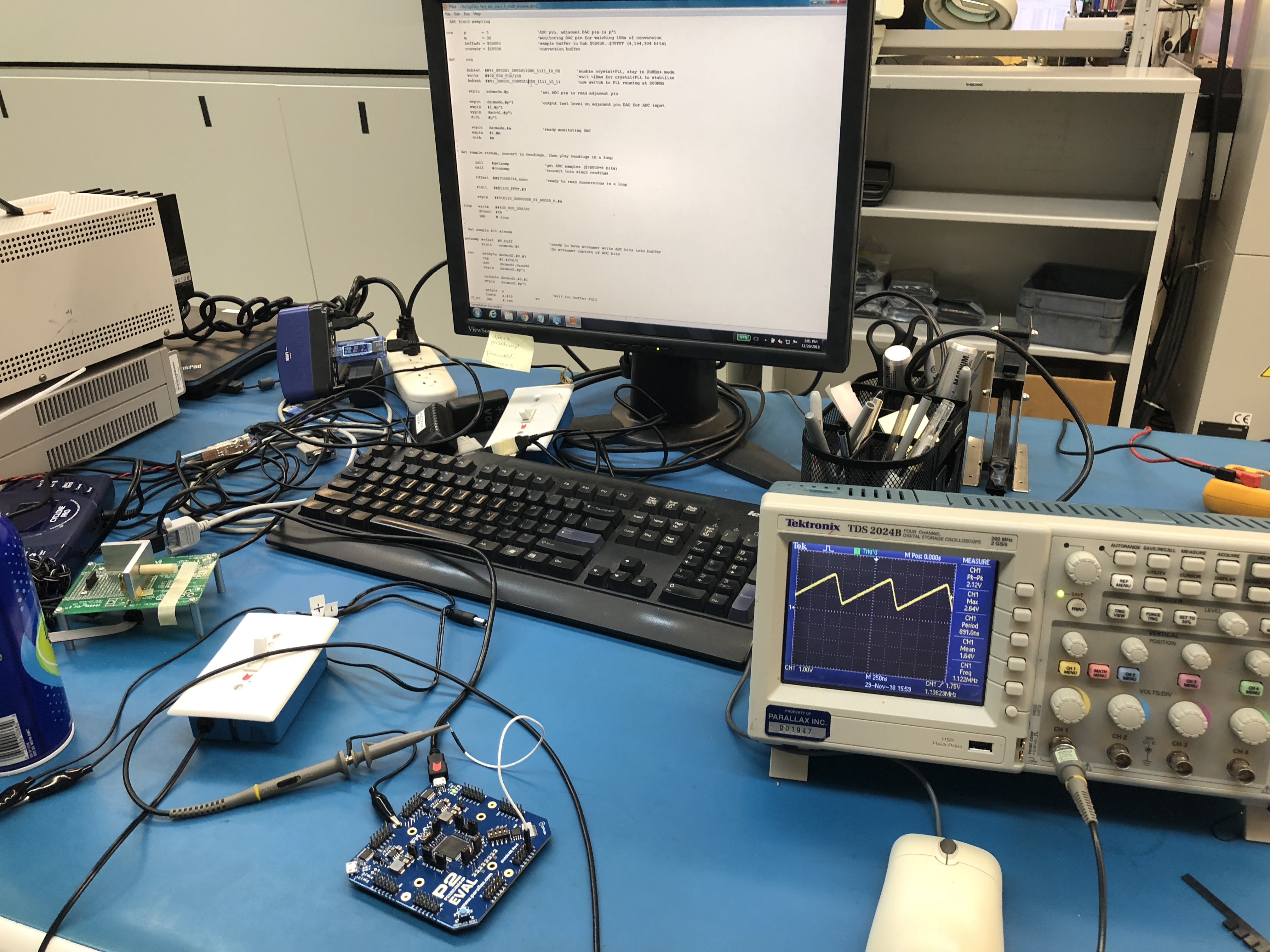
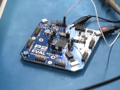
Today, Chip arrived at Parallax to get a look at the P2 Evaluation Boards and for our meeting with ON Semiconductor. The P2 Evaluation Boards need some adjustment on the power supply caps which they'll be making over the next couple of days before we ship these boards to all of you. Switching power supply design is always such a challenge for us and I'm not really sure why, but the engineers will sort it out with a few more Digi-Key drops. We're really close and this isn't a problem for the team. We'll finish the production and send you the boards at some point soon.
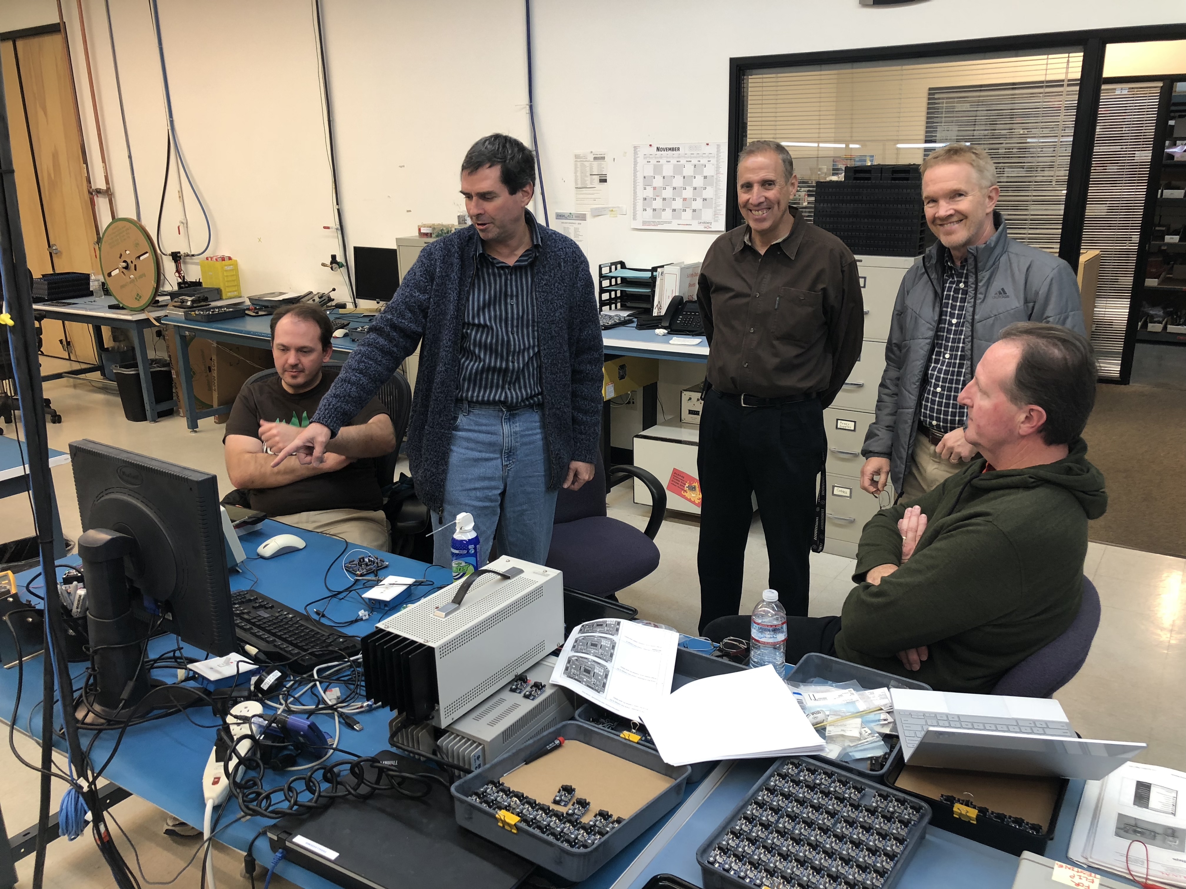
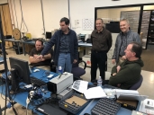
We also showed ON where we are with the project. Chip explained the signal generation, Jeff froze the board with freon (?) and David heated it up. Then we sat down to discuss:
- schedule and how it depends on all of us testing the P2 and Chip authorizing the final 13-week restart for final Verilog changes and production
- volume production costs and schedule
- timing and specifications of possible P2 derivatives in the future
- the outstanding financial commitment to achieve this project (no comment)
Should we be able to restart ON the first week of January (and if their key staff is available to support us) we could have chips the second week of April. This could enable a Spring Propeller Expo at Parallax, but it's feeling awfully tight at this time. It's starting to feel like Fall 2019 is the right time for the event because summer heat is miserable in Rocklin. The Parallax team has also worked tirelessly to fuel the project and looks forward to completion.
Thanks for all of your support!
Ken Gracey


Comments
That photo with Chip explaining something to the group is great! Jeff sitting there arms folded and with a stern look at Chip appears to be thinking "yeah yeah Chip, now when do you get to the software/tools?" (I know Jeff is too nice for that, but it just looks like it.)
Chip looks happy! It's all starting to happen!
@Ken, thanks for the pictures. No worries, at least for me, regarding finalizing everything. I'm happy to wait for it to be as solid as possible.
Expo on the later schedule makes great sense. Second you on the heat!
Man, I have to say I am really looking forward to that. Seeing everyone again. It's been too darn long.
You know, what I really want to know is what the guys at On think about all this! Chip seems to be squeezing a lot out of this process. Would be awesome to get those guys a couple beers and their take on this P2 saga.
I'm marking up a schematic of one of my bare P1-based S-100 homebrew computer boards, to accept a DIP->ribbon cable adapter to the Eval board instead of the P1. Hope to have that ready when the Eval board arrives. Need to rearrange some projects in my office this weekend to make room!
Well spotted ! - wait, there are two of them on that bench !
1) The 10-bit VCO divider is faster, after all, than the VCO. It always keeps up with the VCO and reveals the VCO speed limits.
2) The VCO tops out around 400MHz at room temp, but then slows as heat builds.
3) At cold temperatures, the core logic can run faster than the VCO. The VCO is the limiter. We had the core logic running at 422MHz, briefly.
4) At very high core speeds, the I/O pads have set-up time problems in clocked modes.
5) We were able to run the P2 at 300MHz and push the temperature to 115C with a heat gun, before we started experiencing set-up time problems in the I/O pads. So, 300MHz seems like a conservative overclocking speed.
6) The P2 Eval board, with its many bypass caps and good heat dissipation, allows the performance envelope to be pushed pretty far.
7) ADC activity seems less noisy.
That's all pretty darn good news! Great to hear!
The eval board is good for evaluating the P2 chip itself and pushing the limits whereas the P2D2 module can be plugged directly into your system, so it is better for embedding and much smaller. Plus the headers are more suitably arranged even for ribbon cable.
These are great results, congratulations. Above 400 MHz if only briefly is stunning.
We've also seen that VCO droop as it gets hotter, but at lower clock rates. I suspect that has to do with getting the heat away quickly enough
As soon as we can, it would be good to obtain ADC statistical data and/or streams across pins
Very Good results, especially around VCO and PLL limits, and to me, makes a compelling case to make the next P2D2 a 4 layer design.
2 layer versions can always be done in the future, right now the supply of chips is very constrained, so silicon testing should take priority over PCB variants testing.
I'll put my name down for a 4 Layer 3Amp* SMPS P2D2
* Current drain numbers seem to bump the 'best fit' SMPS on P2D2 to a higher current model ?
I get this modeling for reaching (if briefly) 440MHz test points ie > 1.8A regulator ability needed.
Vcc=1.8;Cpd=1.60n+8*83.33p = 2.26664e-9 Fi=440M
Id = Cpd * Vcc * Fi + 5m Id = 1.80017888A
ie 1A is clearly not enough, 2A may be just ok, 3A has margin.
I see Mouser & Digikey both now have stocks of MPM3632C ( 3A integrated inductor QFN-20 3mmx5mmx1.6mm )
Was that rough indicator of ADC activity seems less noisy, running with SMPS 3v3, or the low noise 3v3 regulators ?
Does the better/proper package have better GND pad bonding ?
Once the P2D2 module becomes available to mere mortals, I'd like to purchase one. Although a recent post said that around 15 packaged test chips were headed your way, it seems likely that they won't cover the early demand from tool makers for your board (unless they go the evaluation board route). But if you do happen to find yourself with a spare populated board that you're willing to part with--or if you are trying to justify whether it's prudent to fabricate a batch--I'd be happy to take one off your hands. Meanwhile, I'm sitting on my hands waiting for the tool makers and so on to have first dibs at the Evaluation Board for its limited run.
Anyway, whether the P2 is on the Evaluation Board or on the P2D2 module, there's some PBJ code in the firmware just waiting to come forth (yeah, pun intended). And once the P2 is well characterized and re-spun, I hope that both the Evaluation Board and the P2D2 will be available through Parallax, perhaps the latter being drop-shipped from you. Naturally, the official and very robust Parallax Evaluation Board should have a long life ahead of it (once the P2 goes into production), but the P2D2 is also an evaluation board in its own right.
Looking forward to see the ADC results with a quieter power supply.
Hi ErNa
For a good jump-start, IMHO, you could grab a copy of Marwan AI-Akaidi's book, "Fractal Speech Processing".
https://amazon.de/Fractal-Speech-Processing-Marwan-Al-Akaidi/dp/051175454X
You can walk thru it in two ways, your choice of wich is better for a first approach: it has both comprehensive maths explanations and a lot of illustrative graphs, very learn-friendly.
Hope it helps.
Henrique
I notice the SCH shows 4.7uF caps, in all decoupling points.
Would be worthwhile to compare that scheme, with smaller (eg) 22nF 0402 decoupling on VDD, as the 22nF parts have a lower impedance at higher frequencies.
(~22nF/0402 seems to be a price-package minimum currently)
With SysCLK + analog + PLL + SMPS all in the mix, it's not easy to know which frequency matters most, but it seems the SysCLK spikes from the P2 itself, are best decoupled as close to P2 as possible.
SMPS spikes are best managed closest to the SMPS chip.
0402 also means CAPs can be closer to the pins, for less inductance.
Examples: (I think C5 is a typo and they mean 10nF not 10nH)
@W9GFO - looks like a switch. ;-)
But, perhaps I was too busy drooling over the two boxes of Power Pals next to Jeff!
That sounds great!
Jmg, thanks for posting this. It looks like smaller caps on VDD might be way better.
Something I don't understand, though... The chart bottoms out at around -4.00e+1. Is that really -40 ohms? Is that due to the LC reactance of the the cap? The Y axis doesn't fully make sense to me.
I'm not in the office today- was thinking about overlaying the data on jmg's graph, but I'm not finding that a simple task by phone.:)
The caps were selected not only for decoupling, but also to provide some bulk capacitance distributed around the board, rather than loading that up by the voltage sources.
If even better decoupling performance is required for (I guess) analog resolution, then perhaps alternating the caps around P2-EVAL could be an option.
Maximum expected frequency and at what current? 5ns comes to mind.
Maximum allowable voltage drop (... square root of diddly-squat I hear you say?)
Has actual current performance of 1V8 been measured yet.... I guess that has been done in the long thread....
That's another typo. The DOC came from TI, but it seems was not well proof read.
The Y axis will be a log scale, as these are always log-log graphs, see the pdf above of the 4u7 caps, for the correct Y axis labels.
There is also the PCB ground plane to add, IIRC someone mentioned 1.5nF ?
Yes, it may be experimental. The TI linear voltage regulators likely also have some minimum CL spec.
You mean on the Eval Board - not that I've seen, but you can use the MHz and Cpd numbers to model the expected Icc. I got appx 1.8A at Chip's highest test values.
Just remembering: Amkor's datasheet for the selected LQFP-100 package shows a series inductance of 2.57 nH at the pads near the center of each side, and 3.32 nH at the ones near the corners.
Amkor's data only shows the inductance due to the padframe itself; the series inductance added by the gold wires is not available yet, because it also deppends on the distance each gold wire needs to travel, from the connection point at the padframe, to its destination connection point, at P2 silicon pad ring.
Considering the above and looking only at VDD, if one ever intends to try the 10 nF caps, perhaps the best places would be at the pins near the center of each side (14, 38, 64, 88), then extend its uses towards the corners, if ever needed, to verify if it could improve noise figures or not.
As for VIO, except from V2831 (pin 47, just near to one of the corners), used by the internally-regulated VCO power supply, wich perhaps could benefit from extra covering against high frequency noise coupling, eventually the other pins could also be tested, on a case-by-case basis.
I've done it in the past, using thru-hole mounted multilayers, trying to clean up some pesky switching noise sources, but I don't know if those chip capacitors could be piggybacked, other than by trying to hand solder the 100 nF, on top of the 10 nF ones.
Eventually, that trick can remedy some really bad situation, untill a better solution can be found.