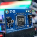
P2D2 Bill of Materials?
 Ken Gracey
Posts: 7,420
Parallax is a proud holder of six (6) bare P2D2 boards. Thanks Peter!
P2D2 is such a fun name, BTW.
I need to prepare to have these built before Chip receives chips.
Where is the Bill of Materials for this board?
Thanks,
Ken Gracey
P2D2 is such a fun name, BTW.
I need to prepare to have these built before Chip receives chips.
Where is the Bill of Materials for this board?
Thanks,
Ken Gracey


Comments
I hate getting things for free... please make enough to sell me 4.
Rich
Would you need paste info for this step, to make a low cost paste screen ?
Does the paste info change across versions here ? - Seems a little care will be needed to keep Assembly Paste + PCBs in step ?
What are 'few more options' ?
Seems we should have a stencil to make our efforts a bit more productive, but I'll ask the people who actually do the work.
Ken Gracey
The other improvements are:
"R6" jumper link can either connect serial header 5V (my enhanced Prop Plug supplies power) to regulator VCC or connect serial header to 3.3V regulator.
SPI Flash footprint can also accommodate the higher capacity devices in the wider .208" packages.
EDIT - Here's a Google spreadsheet that I will keep up to date.
I'm filling in details for the BOM still but this is what I've got at present: (use the Google spreadsheet version now)
Prices on these keep falling, to make them almost a non-brainer....
I see this comment here
"4)Electropolishing : Electropolishing (also known as electrochemical deburring) will remove small burrs, improve surface quality and provide smooth inside walls for better paste release.
This treatment is mainly for IC lead width less than 0.5mm and BGA chips." <<<
FYI
http://smt.iconnect007.com/index.php/article/43313/laser-cut-electropolish-and-laser-cut-nanocoat-stencils-a-comparison-of-finish-performance-for-complex-designs/43316/?skin=smt