P2 PCB - conducting heat out on top layer
 Tubular
Posts: 4,774
in Propeller 2
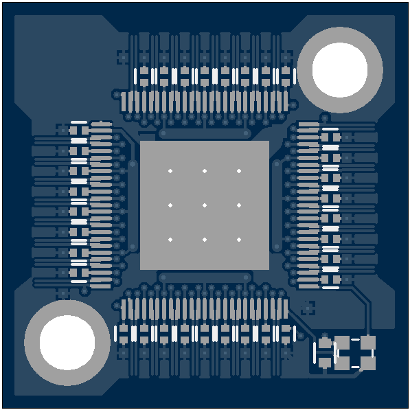
I'm working on a pcb layout and seeing whether we can't conduct heat out on the top layer, via the corners of the QFP.
This involves breaking the 1v8 ring in places so the ground pour can escape at the corners. Thats not a big problem because it can go on the bottom layer along with a 3v3 ring. But its the top layer that really lets the heat escape rather than fester.
The two large holes are solder nut supports (Pemnet SMTSO) for an option 25mm fan, if required.
Heres the layout so far


Comments
eg less than 1oz to 2oz, and less than moving from 2L to 4L PCB
Putting in more vias, and expanding the pour on the bottom side yields many parallel heat pathways.
( eg Peter has 49 vias in the P2D2 layout )
I like the Fan idea... for those who want to overclock the P2
I often incorporate fans in my designs despite being sealed units and having "fanless" components - there are a lot of benefits to recirculating the air despite them being a closed system. From the outside, unless you press your ear to the housings, you hardly hear the fans running.
We have a thermal camera. I reckon there may end up being a 20 degree drop across those corner bottlenecks at peak loading (it depends also on how much the top black surface of the qfp radiates), but that might still be ok. We'll find out soon.
I would think that a stepper wouldn't have much in the way of I/O so there is not much to route but with 64 I/O you would want to route mostly to the same side, so in effect the bottom becomes the top upside down.
@tubular - you've put very very small caps on every power pin which seems excessive and awkward for manual assembly. I just use 0603s and there is still a lot of them, probably way more than we really need but I've allowed for them anyway. If the interconnection between the power pins are low impedance then it doesn't need individual caps. Imagine if P2 had 4 I/O power and 4 CPU power pins, we wouldn't stack 4 caps on each pin, just 8 total.
Mount it so the heat pad connects to the metal box sideways/top would get a lot of heat away.
Touching what is the via side (bottom) but large c-spring touching the top of the part helps too.
Fan and moving parts is not reliable for 10years.
They make dual side mosfet now, so you can cool from the top:
https://www.mouser.com/ProductDetail/Vishay-Siliconix/SIDR680DP-T1-GE3?qs=sGAEpiMZZMshyDBzk1/Wi/D7Em5shE8qPi5iyfn4eIkJa/go3OZA%2bA==
https://www.mouser.com/ProductDetail/STMicroelectronics/STLD125N4F6AG?qs=sGAEpiMZZMshyDBzk1/Wi89zNAzMDMhysu7TQcLuxMzjl84xoxvYrw==
This sounds like a comment based on cheap computer fans designed to keep you upgrading.
If you look at the specs on quality (eg) ebm papst fans you'll see many models that have L10 figures well over 10 years. If you go by IPC L10 figures, many approach 20 years, and L10 means 90% of them continue operating past that point.
Once we get past prototyping this will be placed on a board which already has over 400 part placements and we're really not going to notice the small addition.
During proto of course we don't need to load everything up, but if we want a blend of cap values to suppress a wider spectrum then we have the pcb pad flexibility to do so.
Our initial focus will be on the analog performance of the pins
This one might edge-solder direct to the via-array, for bottom-side radiator ?
or these also bottom side solder...
and this may have 2 possible solder attach - either way up, inverted could solder one side to via-area, needing another offset pad for stability.
or larger are these LED coolers, quite impressive, with a 6 holes Dia 25.4mm and a solid looking core. A ceramic or copper spacer would lift this off the pcb plane, via side.
A search on ebay for Aluminum Heatsink with fan for 5W/10W High Power LED Cooling
finds some models, L58xW54xH14mm
Tony, nice find on the double sided FET. I hadn't seen those before
https://www.mouser.com/ProductDetail/Toshiba/TB67B000FGEL?qs=sGAEpiMZZMtKB4wrjsn3laYUYxNRg6Sfiz6gwzdjW48=
hehe, maybe if someone wants to push it to the Liquid Nitrogen over-clocking space ?
I doubt that package top-slug comes standard in ETQFP100, and the P2 power envelope is not double-digit watts.
Things like 2oz or 3oz copper and 4Layer pcbs are likely to be cheaper heat-spreading solutions.
Even without a top-slug, you can still top-cool - there are RasPi examples of top-cooling via the plastic package
Heatsinks like Sunon SA000-12016 or SA000-12024 come with 0.25mm thermal sticky pads, so could apply both top and bottom cooling.
They assumed a 5x5 via array on the thermal pad land, going down to an internal ground plane that was 2x2". That was sufficient, but if you think about it, that's a lot of accommodation to make.
-Phil
It may not be too bad, it'd be like the DE0-Nano footprint we're already used to.
Here's roughly what it'd look like with DE0-Nano header spacing. Plenty of space for an FT2232H (high speed, dual port). It could be longer like the DE0-Nano, which is around 3x2" size, to get a true 4 square inch copper plane.
which is why... Yup. Two of the examples I gave are tinned copper and the third one, is tin plated Aluminium, designed to be soldered.
That's getting quite custom - there are plenty of RaspPi heatsinks out there, that usually come 14x14, 10x10 finned and a smaller copper one, so nicely do the P2 Top and P2 Via areas, with sticky thermal pads.
Not as conducting as solder, but very easy to get and apply.
I would use 2Oz copper first.
I stick fans on lots of one-off pieces of equipment, including the cheap MagicJack+ we depend on for our home phone. Thermally, the MJ+ is a complete piece of trash. So is its power supply. But they will last forever with a bit o' cooling.
http://www.ti.com/lit/an/slma002h/slma002h.pdf
They have a lot more vias… 0.3 mm dia. with 1.5 mm pitch, looks like...
For the footprint, look for PLQP0100KD-A at page 32 of the following-linked pdf document.
https://www.renesas.com/br/en/doc/products/others/r50zz0003ej0700_package.pdf
Also pay especial attention to the "Notes on Mounting Pad Design for HQFP and HLQFP Mounting", figures 5.33 and 5.34 at page 124 of the same document. They show how to avoid the possibility of solder influx under the package, during assembly.
It seems to nicely fit Tubular's previously posted layout, perhaps with some minor tweaks.
For Peter Jakacki's previously posted options, one could use a suitable side-cutting plier, and completely remove the four extra leads, before soldering the package onto the pcb.
Henrique
That link had issues loading, but I found a single-page pdf here, of the suggested copper areas that most can infer from
https://www.renesas.com/cn/zh/package-image/pdf/mountpad/fig1015e.pdf
Interesting idea - I wonder how much gain those corner wings would give, over the already large thermal pad P2 uses.
The big thermal pad, is directly 'parallel path' down from the die, whilst the corner wings are 'series path', lead frame-thin.
Google suggests there is a QFN100 package, which could be smaller and there is even a small-volume vendor of this
http://www.mirrorsemi.com/OpenChip.html
Mentions a 10.2mm Pad/die, - what was the final die size of the P2 ? - could the P2 fit into this cavity ?
The FT90x series have QFN100 offerings (but with slightly smaller pad size) and the price of FT90x suggests the QFN is cheaper than non-thermal TQFP100 ?
Capacitors won't conduct heat so well, so I'd put them a bit further out...
If the P2 lacked any E-PAD, I'd agree. (tho caps further out increase the decoupling inductance)
However, with the E-PAD, the vast majority of heat flow will be straight down, skinny gull leads long-ways, are not going to conduct heat well.
The trick then is to spread that straight-down heat flow, to fan-out.
Peter's PCB does that well, with radiating GND areas, but 2oz or 4 layers will also help.
Doing early P2 boards in 4 layers first, and then drop layers as the part is proven, could also make sense. Decoupling caps on underside can also be much shorter paths.
This layout looks really good to me.
I believe I've got it (the reason for the link not working, when accessed from other systems/browsers).
It was my fault, indeed, because I had the same difficulty when I've tried to transpose the link from one of my computers to the other one, but I've relegated it to the "mistyping" kind, and restarted the search path at the second system.
If you google-it by using the document name "r50zz0003ej0700_package.pdf" as the search term, it will not work, as it had occured to me, before.
- So, step by step-wise:
- Start at: https://www.renesas.com/us/en/
- Into the Search box, type: Semiconductor Package Mount Manual
- Click at the Loupe icon or hit Enter
- When the Keyword-search list is displayed, scroll down to "Documents (1)"
- The link to the document that will work for you appears in blue, followed by a grey line containing:
May.30.16 | Rev.7.00 | 10.42 Mbytes | r50zz0003ej0700 | Common Item
Sure, it worths reading.
Henrique
Yes, I started nudging them outwards a little bit (the top left and bottom right in layout has them further out, compared with (minimum) top right and lower left, and since them I've moved them a little further out
At first thought, I surely would agree with you.
Thinking a bit further, perhaps the term "parallel path" couldn't really be aplied, when it comes to the exposed pad situation itself.
I'll try to explain what leaded me to the above conclusion.
When the image of this specific package appeared, as a result of one of the many search terms I'd used yesterday, I also wondered "What reason does Renesas designers had in mind, to use that specific package?", "Why they didn't agreed to solely (and simply) depend on the huge exposed pad (aka, thermal paddle).
As it occured, at least to me, the word "THERMAL" floated-up, inside my mind, as heat flowing out of a barbecue cast iron plate.
- Heat increases the temperature, hence enlarges exposed pad physical dimensions and also its resistance;
- The maximum effects occurs right there, at the thermal pad, that is inserted between the chip and pcb's GND plane, hence in series with die's GND connections;
- Due to Skin Effect, AC currents would experience an easier flow path, contouring the exposed pad, near its surface, than right thru its thickness;
- The hotter the exposed pad, the larger the path that currents have to flow, before reaching the silicon die;
- The immediately underneath copper GND plane region, to wich the exposed pad is attached with solder, also suffers from the same effects, due to temperature raise;
- In fact, despite the longer path and the intrinsically associated series-indutance, due to their lenght and shape, the four "extra" conductors, being slightly cooler that the thermal pad itself, tend to help a bit, decreasing the total effective series resistance GND AC current paths would experience, when flowing to serve the internally-connected semiconductor needs.
- As a probable bonus, those metal protrusions are part of the "scrapped" material, that need to be sawed-out, before the other leads are formed, to their final shapes. So, it's unlikely that they'll represent a significant increase in package cost.
Last (but not least) if God had given to me at least a chance, to choose between having or not having six functional fingers in each hand, and also six functional toes in each foot, my answer would surely be "Don't toss them out, please!".
Further good references could also be found at:
https://pcbcart.com/article/content/PCB-internal-thermal-dissipation-design.html
I hope this time the link works, at least!
Henrique